- 您現在的位置:買賣IC網 > PDF目錄374037 > ADSP-BF561SKBCZ500 (ANALOG DEVICES INC) Blackfin Embedded Symmetric Multi-Processor PDF資料下載
參數資料
| 型號: | ADSP-BF561SKBCZ500 |
| 廠商: | ANALOG DEVICES INC |
| 元件分類: | 數字信號處理 |
| 英文描述: | Blackfin Embedded Symmetric Multi-Processor |
| 中文描述: | 32-BIT, 500 MHz, OTHER DSP, PBGA256 |
| 封裝: | 12 X 12 MM, ROHS COMPLIANT, MO-225, BGA-256 |
| 文件頁數: | 13/52頁 |
| 文件大小: | 508K |
| 代理商: | ADSP-BF561SKBCZ500 |
第1頁第2頁第3頁第4頁第5頁第6頁第7頁第8頁第9頁第10頁第11頁第12頁當前第13頁第14頁第15頁第16頁第17頁第18頁第19頁第20頁第21頁第22頁第23頁第24頁第25頁第26頁第27頁第28頁第29頁第30頁第31頁第32頁第33頁第34頁第35頁第36頁第37頁第38頁第39頁第40頁第41頁第42頁第43頁第44頁第45頁第46頁第47頁第48頁第49頁第50頁第51頁第52頁
ADSP-BF561
Preliminary Technical Data
Rev. PrC
|
Page 13 of 52
|
April 2004
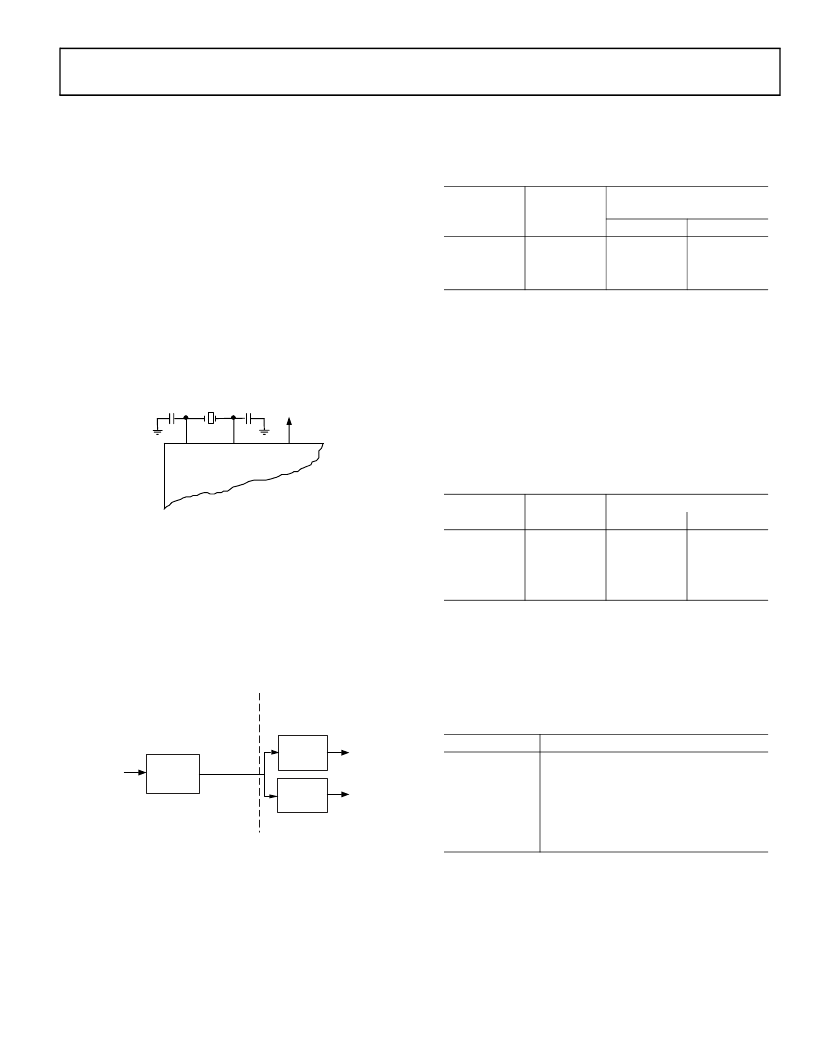
CLOCK SIGNALS
The ADSP-BF561 can be clocked by an external crystal, a sine
wave input, or a buffered, shaped clock derived from an external
clock oscillator.
If an external clock is used, it should be a TTL compatible signal
and must not be halted, changed, or operated below the speci-
fied frequency during normal operation. This signal is
connected to the processor’s CLKIN pin. When an external
clock is used, the XTAL pin must be
left
unconnected.
Alternatively, because the ADSP-BF561 includes an on-chip
oscillator circuit, an external crystal may be used. The crystal
should be connected across the CLKIN and XTAL pins, with
two capacitors connected as shown in
Figure 5
Capacitor values are dependent on crystal type and should be
specified by the crystal manufacturer. A parallel-resonant, fun-
damental frequency, microprocessor-grade crystal should be
used.
As shown in
Figure 6
, the core clock (CCLK) and system
peripheral clock (SCLK) are derived from the input clock
(CLKIN) signal. An on-chip PLL is capable of multiplying the
CLKIN signal by a user programmable 1x to 63x multiplication
factor. The default multiplier is 10x, but it can be modified by a
software instruction sequence. On-the-fly frequency changes
can be effected by simply writing to the PLL_DIV register.
All on-chip peripherals are clocked by the system clock (SCLK).
The system clock frequency is programmable by means of the
SSEL3–0 bits of the PLL_DIV register. The values programmed
into the SSEL fields define a divide ratio between the PLL output
(VCO) and the system clock. SCLK divider values are 1 through
15.
Table 5
illustrates typical system clock ratios:
The maximum frequency of the system clock is f
SCLK
. Note that
the divisor ratio must be chosen to limit the system clock fre-
quency to its maximum of f
SCLK
. The SSEL value can be changed
dynamically without any PLL lock latencies by writing the
appropriate values to the PLL divisor register (PLL_DIV).
The core clock (CCLK) frequency can also be dynamically
changed by means of the CSEL[1–0] bits of the PLL_DIV regis-
ter. Supported CCLK divider ratios are 1, 2, 4, and 8, as shown
in
Table 6
. This programmable core clock capability is useful for
fast core frequency modifications.
BOOTING MODES
The ADSP-BF561 has three mechanisms (listed in
Table 7
) for
automatically loading internal L1 instruction memory after a
reset. A fourth mode is provided to execute from external mem-
ory, bypassing the boot sequence.
Figure 5. External Crystal Connections
Figure 6. Frequency Modification Methods
CLKIN
CLKOUT
XTAL
PLL
1
×
- 63
×
×
1:15
×
1, 2, 4, 8
VCO
SCLK
≤
CCLK
SCLK
≤
133MHZ
CLKIN
“FINE” ADJUSTMENT
REQUIRES PLL SEQUENCING
“COARSE” ADJUSTMENT
ON-THE-FLY
CCLK
SCLK
Table 5. Example System Clock Ratios
Signal Name
SSEL[3–0]
Divider Ratio
VCO/SCLK
Example Frequency Ratios
(MHz)
VCO
100
300
500
SCLK
100
50
50
0001
0110
1010
1:1
6:1
10:1
Table 6. Core Clock Ratios
Signal Name
CSEL[1–0]
Divider Ratio
VCO/CCLK
Example Frequency Ratios
VCO
500
500
200
200
CCLK
500
250
50
25
00
01
10
11
1:1
2:1
4:1
8:1
Table 7. Booting Modes
BMODE1–0
00
Description
Execute from 16-bit external memory (Bypass
Boot ROM)
Boot from 8/16-bit flash
Reserved
Boot from SPI serial ROM (16-bit address
range)
01
10
11
相關PDF資料 |
PDF描述 |
|---|---|
| ADSP-BF561 | Synchronous 4-Bit Up/Down Binary Counters With Dual Clock and Clear 16-PDIP 0 to 70 |
| ADSP-BF561SBB500 | Blackfin Embedded Symmetric Multi-Processor |
| ADSP21020 | 32/40-Bit IEEE Floating-Point DSP Microprocessor |
| ADSP-21020BG-100 | 32/40-Bit IEEE Floating-Point DSP Microprocessor |
| ADSP2184 | 16 A SPDT MINIATURE POWER RELAY |
相關代理商/技術參數 |
參數描述 |
|---|---|
| ADSP-BF561SKBCZ-5A | 功能描述:IC DSP CTLR 32BIT BKFN 256CSPBGA RoHS:是 類別:集成電路 (IC) >> 嵌入式 - DSP(數字式信號處理器) 系列:Blackfin® 標準包裝:40 系列:TMS320DM64x, DaVinci™ 類型:定點 接口:I²C,McASP,McBSP 時鐘速率:400MHz 非易失內存:外部 芯片上RAM:160kB 電壓 - 輸入/輸出:3.30V 電壓 - 核心:1.20V 工作溫度:0°C ~ 90°C 安裝類型:表面貼裝 封裝/外殼:548-BBGA,FCBGA 供應商設備封裝:548-FCBGA(27x27) 包裝:托盤 配用:TMDSDMK642-0E-ND - DEVELPER KIT W/NTSC CAMERA296-23038-ND - DSP STARTER KIT FOR TMS320C6416296-23059-ND - FLASHBURN PORTING KIT296-23058-ND - EVAL MODULE FOR DM642TMDSDMK642-ND - DEVELOPER KIT W/NTSC CAMERA |
| ADSP-BF561SKBCZ-5V | 功能描述:IC DSP 32BIT 500MHZ 256CSPBGA RoHS:是 類別:集成電路 (IC) >> 嵌入式 - DSP(數字式信號處理器) 系列:Blackfin® 標準包裝:2 系列:StarCore 類型:SC140 內核 接口:DSI,以太網,RS-232 時鐘速率:400MHz 非易失內存:外部 芯片上RAM:1.436MB 電壓 - 輸入/輸出:3.30V 電壓 - 核心:1.20V 工作溫度:-40°C ~ 105°C 安裝類型:表面貼裝 封裝/外殼:431-BFBGA,FCBGA 供應商設備封裝:431-FCPBGA(20x20) 包裝:托盤 |
| ADSP-BF561SKBCZ600 | 制造商:Analog Devices 功能描述:DSP FIX PT 16BIT 600MHZ 600MIPS 256CSPBGA - Trays 制造商:Analog Devices 功能描述:IC MULTI-PROCESSOR |
| ADSP-BF561SKBCZ-6A | 功能描述:IC DSP CTRLR 32B 600MHZ 256CPBGA RoHS:是 類別:集成電路 (IC) >> 嵌入式 - DSP(數字式信號處理器) 系列:Blackfin® 標準包裝:40 系列:TMS320DM64x, DaVinci™ 類型:定點 接口:I²C,McASP,McBSP 時鐘速率:400MHz 非易失內存:外部 芯片上RAM:160kB 電壓 - 輸入/輸出:3.30V 電壓 - 核心:1.20V 工作溫度:0°C ~ 90°C 安裝類型:表面貼裝 封裝/外殼:548-BBGA,FCBGA 供應商設備封裝:548-FCBGA(27x27) 包裝:托盤 配用:TMDSDMK642-0E-ND - DEVELPER KIT W/NTSC CAMERA296-23038-ND - DSP STARTER KIT FOR TMS320C6416296-23059-ND - FLASHBURN PORTING KIT296-23058-ND - EVAL MODULE FOR DM642TMDSDMK642-ND - DEVELOPER KIT W/NTSC CAMERA |
| ADSP-BF561SKBCZ-6A | 制造商:Analog Devices 功能描述:Digital Signal Processor IC |
發布緊急采購,3分鐘左右您將得到回復。