- 您現在的位置:買賣IC網 > Datasheet目錄39 > ADT7518ARQZ (Analog Devices Inc)IC SENSOR TEMP QD ADC/DAC 16QSOP Datasheet資料下載
參數資料
| 型號: | ADT7518ARQZ |
| 廠商: | Analog Devices Inc |
| 文件頁數: | 18/40頁 |
| 文件大小: | 891K |
| 描述: | IC SENSOR TEMP QD ADC/DAC 16QSOP |
| 標準包裝: | 98 |
| 功能: | 溫度監控系統(傳感器) |
| 傳感器類型: | 內部和外部 |
| 感應溫度: | -40°C ~ 120°C,外部傳感器 |
| 精確度: | ±3°C(最小值) |
| 拓撲: | ADC,比較器,多路復用器,寄存器庫 |
| 輸出類型: | I²C?,MICROWIRE?,QSPI?,SPI? |
| 輸出警報: | 無 |
| 輸出風扇: | 無 |
| 電源電壓: | 2.7 V ~ 5.5 V |
| 工作溫度: | -40°C ~ 120°C |
| 安裝類型: | 表面貼裝 |
| 封裝/外殼: | 16-SSOP(0.154",3.90mm 寬) |
| 供應商設備封裝: | 16-QSOP |
| 包裝: | 托盤 |
| 產品目錄頁面: | 798 (CN2011-ZH PDF) |
第1頁第2頁第3頁第4頁第5頁第6頁第7頁第8頁第9頁第10頁第11頁第12頁第13頁第14頁第15頁第16頁第17頁當前第18頁第19頁第20頁第21頁第22頁第23頁第24頁第25頁第26頁第27頁第28頁第29頁第30頁第31頁第32頁第33頁第34頁第35頁第36頁第37頁第38頁第39頁第40頁
ADT7518
Rev. A | Page 18 of 40
The ADT7518 powers up with averaging on. This means every
channel is measured 16 times and internally averaged to reduce
noise. The conversion time can also be sped up by turning off
the averaging. This is done by setting Bit C5 of the Control
Configuration 2 register (Address 19h) to 1.
FUNCTION DESCRIPTIONVOLTAGE OUTPUT
Digital-to-Analog Converters
The ADT7518 has four resistor string DACs fabricated on a
CMOS process with resolutions of 12, 10, and 8 bits, respec-
tively. They contain four output buffer amplifiers and are
written to via I
2
C serial interface or SPI serial interface. See
the Serial Interface section for more information.
The ADT7518 operates from a single supply of 2.7 V to 5.5 V,
and the output buffer amplifiers provide rail-to-rail output
swing with a slew rate of 0.7 V/祍. All four DACs share a com-
mon reference input, VREF-IN. The reference input is buffered to
draw virtually no current from the reference source because it
offers the source a high impedance input. The devices have a
power-down mode in which all DACs may be turned off
completely with a high impedance output.
Each DAC output will not be updated until it receives the
LDAC command. Therefore, while the DAC registers would
have been written to with a new value, this value will not be
represented by a voltage output until the DACs have received
the LDAC command. Reading back from any DAC register
prior to issuing an LDAC command will result in the digital
value that corresponds to the DAC output voltage. Thus, the
digital value written to the DAC register cannot be read back
until after the LDAC command has been initiated. This LDAC
command can be given by either pulling the LDAC
pin low
(falling edge loads DACs), setting up Bits D4 and D5 of the
DAC configuration register (Address 1Bh), or using the LDAC
register (Address 1Ch).
When using the LDAC
pin to control the DAC register loading,
the low going pulse width should be 20 ns minimum. The
LDAC
pin has to go high and low again before the DAC
registers can be reloaded.
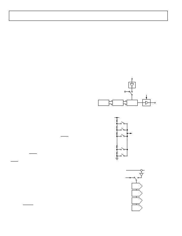
Digital-to-Analog Section
The architecture of one DAC channel consists of a resistor
string DAC followed by an output buffer amplifier. The voltage
at the VREF-IN pin or the on-chip reference of 2.25 V provides
the reference voltage for the corresponding DAC. Figure 38
shows a block diagram of the DAC architecture. Since the input
coding to the DAC is straight binary, the ideal output voltage is
given by
N
REF
OUT
D
V
V
2
?/DIV>
=
where:
D = decimal equivalent of the binary code that is loaded to the
DAC register:
0 to 255 for ADT7518 (8 bits)
N = DAC resolution
Resistor String
The resistor string section is shown in Figure 39. It is simply a
string of resistors, each of approximately 603 &. The digital
code loaded to the DAC register determines at which node on
the string the voltage is tapped off to be fed into the output
amplifier. The voltage is tapped off by closing one of the
switches connecting the string to the amplifier. Because it is a
string of resistors, it is guaranteed monotonic.
INPUT
REGISTER
DAC
REGISTER
RESISTOR
STRING
V
OUT
-A
OUTPUT BUFFER
AMPLIFIER
GAIN MODE
(GAIN = 1 OR 2)
REFERENCE
BUFFER
INT V
REF
V
REF
-IN
Figure 38. Single DAC Channel Architecture
R
R
R
R
R
TO OUTPUT
AMPLIFIER
Figure 39. Resistor String
STRING
DAC A
2.25V
INTERNAL V
REF
V
REF
-IN
STRING
DAC B
STRING
DAC C
STRING
DAC D
Figure 40. DAC Reference Buffer Circuit
相關PDF資料 |
PDF描述 |
|---|---|
| AT30TS00-MAH-T | SENSOR DGTL TEMP I2C/SMBUS 8WDFN |
| AT30TSE002B-MAH-T | SENSOR DGTL TEMP I2C/SMBUS 8WDFN |
| BD3504FVM-TR | IC REG CTRLR SGL POS ADJ 8MSOP |
| BD3521FVM-TR | IC REG CTRLR SGL 1.5V MSOP8 |
| BD9153MUV-E2 | IC REG TRPL BCK/LINEAR 24VQFN |
相關代理商/技術參數 |
參數描述 |
|---|---|
| ADT7518ARQZ-REEL | 制造商:Analog Devices 功能描述:Temp Sensor Analog Serial (4-Wire, SPI, I2C) 16-Pin QSOP T/R |
| ADT7518ARQZ-REEL7 | 制造商:Analog Devices 功能描述:Temp Sensor Analog Serial (4-Wire, SPI, I2C) 16-Pin QSOP T/R |
| ADT7519 | 制造商:AD 制造商全稱:Analog Devices 功能描述:SPI-/I2C-Compatible, Temperature Sensor,4-Channel ADC and Quad Voltage Output |
| ADT7519ARQ | 制造商:Analog Devices 功能描述:Temp Sensor Digital Serial (4-Wire, SPI, I2C) 16-Pin QSOP |
| ADT7519ARQ-REEL | 制造商:Analog Devices 功能描述:Temp Sensor Digital Serial (4-Wire, SPI, I2C) 16-Pin QSOP T/R |
發布緊急采購,3分鐘左右您將得到回復。