- 您現(xiàn)在的位置:買賣IC網(wǎng) > Datasheet目錄39 > ADT7518ARQZ (Analog Devices Inc)IC SENSOR TEMP QD ADC/DAC 16QSOP Datasheet資料下載
參數(shù)資料
| 型號(hào): | ADT7518ARQZ |
| 廠商: | Analog Devices Inc |
| 文件頁(yè)數(shù): | 9/40頁(yè) |
| 文件大小: | 891K |
| 描述: | IC SENSOR TEMP QD ADC/DAC 16QSOP |
| 標(biāo)準(zhǔn)包裝: | 98 |
| 功能: | 溫度監(jiān)控系統(tǒng)(傳感器) |
| 傳感器類型: | 內(nèi)部和外部 |
| 感應(yīng)溫度: | -40°C ~ 120°C,外部傳感器 |
| 精確度: | ±3°C(最小值) |
| 拓?fù)洌?/td> | ADC,比較器,多路復(fù)用器,寄存器庫(kù) |
| 輸出類型: | I²C?,MICROWIRE?,QSPI?,SPI? |
| 輸出警報(bào): | 無(wú) |
| 輸出風(fēng)扇: | 無(wú) |
| 電源電壓: | 2.7 V ~ 5.5 V |
| 工作溫度: | -40°C ~ 120°C |
| 安裝類型: | 表面貼裝 |
| 封裝/外殼: | 16-SSOP(0.154",3.90mm 寬) |
| 供應(yīng)商設(shè)備封裝: | 16-QSOP |
| 包裝: | 托盤 |
| 產(chǎn)品目錄頁(yè)面: | 798 (CN2011-ZH PDF) |
第1頁(yè)第2頁(yè)第3頁(yè)第4頁(yè)第5頁(yè)第6頁(yè)第7頁(yè)第8頁(yè)當(dāng)前第9頁(yè)第10頁(yè)第11頁(yè)第12頁(yè)第13頁(yè)第14頁(yè)第15頁(yè)第16頁(yè)第17頁(yè)第18頁(yè)第19頁(yè)第20頁(yè)第21頁(yè)第22頁(yè)第23頁(yè)第24頁(yè)第25頁(yè)第26頁(yè)第27頁(yè)第28頁(yè)第29頁(yè)第30頁(yè)第31頁(yè)第32頁(yè)第33頁(yè)第34頁(yè)第35頁(yè)第36頁(yè)第37頁(yè)第38頁(yè)第39頁(yè)第40頁(yè)
ADT7518
Rev. A | Page 9 of 40
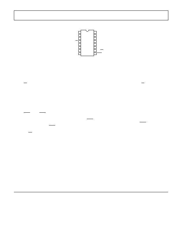
PIN CONFIGURATION AND FUNCTIONAL DESCRIPTIONS
ADT7518
TOP VIEW
(Not to Scale)
V
OUT
-B 1
V
OUT
-C
16
V
OUT
-A 2
V
OUT
-D
15
V
REF
-IN 3
AIN4
14
CS 4
SCL/SCLK
13
GND 5
SDA/DIN
12
V
DD
6
DOUT/ADD
11
D+/AIN1 7
INT/INT
10
D/AIN2 8
LDAC/AIN3
9
Figure 7. Pin Configuration QSOP
Table 5. Pin Function Descriptions
Pin
No. Mnemonic Description
1
V
OUT
-B
Buffered Analog Output Voltage from DAC B. The output amplifier has rail-to-rail operation.
2
V
OUT
-A
Buffered Analog Output Voltage from DAC A. The output amplifier has rail-to-rail operation.
3
VREF-IN
Reference Input Pin for All Four DACs. This input is buffered and has an input range from 1 V to VDD.
4
CS
SPI Active Low Control Input. This is the frame synchronization signal for the input data. When CS
goes low, it enables
the input register, and data is transferred in on the rising edges and out on the falling edges of the subsequent serial
clocks. It is recommended that this pin be tied high to V
DD
when operating the serial interface in I
2
C mode.
5
GND
Ground Reference Point for All Circuitry on the Part. Analog and digital ground.
6
VDD
Positive Supply Voltage, 2.7 V to 5.5 V. The supply should be decoupled to ground.
7
D+/AIN1
D+. Positive Connection to External Temperature Sensor. AIN1. Analog Input. Single-ended analog input channel.
Input range is 0 V to 2.25 V or 0 V to VDD.
8
D/AIN2
D. Negative Connection to External Temperature Sensor.
AIN2. Analog Input. Single-ended analog input channel. Input range is 0 V to 2.25 V or 0 V to V
DD
.
9
LDAC
/AIN3 LDAC
. Active Low Control Input. Transfers the contents of the input registers to their respective DAC registers. A
falling edge on this pin forces any or all DAC registers to be updated if the input registers have new data. A minimum
pulse width of 20 ns must be applied to the LDAC
pin to ensure proper loading of a DAC register. This allows simul-
taneous update of all DAC outputs. Bit C3 of the Control Configuration 3 register enables the LDAC
pin. Default is
with the LDAC
pin controlling the loading of the DAC registers.
AIN3. Analog Input. Single-ended analog input channel. Input range is 0 V to 2.25 V or 0 V to V
DD
.
10
INT/INT
Over Limit Interrupt. The output polarity of this pin can be set to give an active low or active high interrupt when
temperature,VDD, or AIN limits are exceeded. The default is active low. Open-drain outputneeds a pull-up resistor.
11
DOUT/ADD SPI Serial Data Output. Logic output. Data is clocked out of any register at this pin. Data is clocked out on the falling
edge of SCLK. Open-drain outputneeds a pull-up resistor.
ADD. I
2
C Serial Bus Address Selection Pin. Logic input. A low on this pin gives the address 1001 000; leaving it floating
gives the address 1001 010; and setting it high gives the address 1001 011. The I
2
C address set up by the ADD pin is
not latched by the device until after this address has been sent twice. On the eighth SCL cycle of the second valid
communication, the serial bus address is latched in. Any subsequent changes on this pin will have no effect on the
I
2
C serial bus address.
12
SDA/DIN
SDA. I
2
C Serial Data Input/Output. I
2
C serial data to be loaded into the parts registers and read from these registers is
provided on this pin. Open-drain configurationneeds a pull-up resistor.
DIN. SPI Serial Data Input. Serial data to be loaded into the parts registers is provided on this pin. Data is clocked into
a register on the rising edge of SCLK. Open-drain configurationneeds a pull-up resistor.
13
SCL/SCLK
Serial Clock Input. This is the clock input for the serial port. The serial clock is used to clock data out of any register of
the ADT7518 and also to clock data into any register that can be written to. Open-drain configurationneeds a pull-
up resistor.
14
AIN4
Analog Input. Single-ended analog input channel. Input range is 0 V to 2.25 V or 0 V to V
DD
.
15
V
OUT
-D
Buffered Analog Output Voltage from DAC D. The output amplifier has rail-to-rail operation.
16
VOUT-C
Buffered Analog Output Voltage from DAC C. The output amplifier has rail-to-rail operation.
相關(guān)PDF資料 |
PDF描述 |
|---|---|
| AT30TS00-MAH-T | SENSOR DGTL TEMP I2C/SMBUS 8WDFN |
| AT30TSE002B-MAH-T | SENSOR DGTL TEMP I2C/SMBUS 8WDFN |
| BD3504FVM-TR | IC REG CTRLR SGL POS ADJ 8MSOP |
| BD3521FVM-TR | IC REG CTRLR SGL 1.5V MSOP8 |
| BD9153MUV-E2 | IC REG TRPL BCK/LINEAR 24VQFN |
相關(guān)代理商/技術(shù)參數(shù) |
參數(shù)描述 |
|---|---|
| ADT7518ARQZ-REEL | 制造商:Analog Devices 功能描述:Temp Sensor Analog Serial (4-Wire, SPI, I2C) 16-Pin QSOP T/R |
| ADT7518ARQZ-REEL7 | 制造商:Analog Devices 功能描述:Temp Sensor Analog Serial (4-Wire, SPI, I2C) 16-Pin QSOP T/R |
| ADT7519 | 制造商:AD 制造商全稱:Analog Devices 功能描述:SPI-/I2C-Compatible, Temperature Sensor,4-Channel ADC and Quad Voltage Output |
| ADT7519ARQ | 制造商:Analog Devices 功能描述:Temp Sensor Digital Serial (4-Wire, SPI, I2C) 16-Pin QSOP |
| ADT7519ARQ-REEL | 制造商:Analog Devices 功能描述:Temp Sensor Digital Serial (4-Wire, SPI, I2C) 16-Pin QSOP T/R |
發(fā)布緊急采購(gòu),3分鐘左右您將得到回復(fù)。