- 您現在的位置:買賣IC網 > PDF目錄374039 > ADUC842BCP32-3 (ANALOG DEVICES INC) MicroConverter 12-Bit ADCs and DACs with Embedded High Speed 62-kB Flash MCU PDF資料下載
參數資料
| 型號: | ADUC842BCP32-3 |
| 廠商: | ANALOG DEVICES INC |
| 元件分類: | 微控制器/微處理器 |
| 英文描述: | MicroConverter 12-Bit ADCs and DACs with Embedded High Speed 62-kB Flash MCU |
| 中文描述: | 8-BIT, FLASH, 8.38 MHz, MICROCONTROLLER, QCC56 |
| 封裝: | 8 X 8 MM, LEAD FRAME, MO-220VLLD2, CSP-56 |
| 文件頁數: | 29/88頁 |
| 文件大小: | 903K |
| 代理商: | ADUC842BCP32-3 |
第1頁第2頁第3頁第4頁第5頁第6頁第7頁第8頁第9頁第10頁第11頁第12頁第13頁第14頁第15頁第16頁第17頁第18頁第19頁第20頁第21頁第22頁第23頁第24頁第25頁第26頁第27頁第28頁當前第29頁第30頁第31頁第32頁第33頁第34頁第35頁第36頁第37頁第38頁第39頁第40頁第41頁第42頁第43頁第44頁第45頁第46頁第47頁第48頁第49頁第50頁第51頁第52頁第53頁第54頁第55頁第56頁第57頁第58頁第59頁第60頁第61頁第62頁第63頁第64頁第65頁第66頁第67頁第68頁第69頁第70頁第71頁第72頁第73頁第74頁第75頁第76頁第77頁第78頁第79頁第80頁第81頁第82頁第83頁第84頁第85頁第86頁第87頁第88頁
ADuC841/ADuC842/ADuC843
If using the temperature sensor as the ADC input, the ADC
should be configured to use an ADCCLK of MCLK/32 and four
acquisition clocks.
Rev. 0 | Page 29 of 88
Increasing the conversion time on the temperature monitor
channel improves the accuracy of the reading. To further
improve the accuracy, an external reference with low tempera-
ture drift should also be used.
ADC DMA Mode
The on-chip ADC has been designed to run at a maximum
conversion speed of 2.38 μs (420 kHz sampling rate). When
converting at this rate, the ADuC841/ADuC842/ADuC843
MicroConverter has 2 μs to read the ADC result and to store the
result in memory for further postprocessing; otherwise the next
ADC sample could be lost. In an interrupt driven routine, the
MicroConverter would also have to jump to the ADC interrupt
service routine, which also increases the time required to store
the ADC results. In applications where the parts cannot sustain
the interrupt rate, an ADC DMA mode is provided.
To enable DMA mode, Bit 6 in ADCCON2 (DMA) must be set,
which allows the ADC results to be written directly to a 16 MByte
external static memory SRAM (mapped into data memory
space) without any interaction from the core of the part. This
mode allows the part to capture a contiguous sample stream at
full ADC update rates (420 kHz).
Typical DMA Mode Configuration Example
Setting the parts to DMA mode consists of the following steps:
1.
The ADC must be powered down. This is done by ensuring
that MD1 and MD0 are both set to 0 in ADCCON1.
2.
The DMA address pointer must be set to the start address
of where the ADC results are to be written. This is done by
writing to the DMA mode address pointers DMAL, DMAH,
and DMAP. DMAL must be written to first, followed by
DMAH, and then by DMAP.
3.
The external memory must be preconfigured. This consists
of writing the required ADC channel IDs into the top four
bits of every second memory location in the external
SRAM, starting at the first address specified by the DMA
address pointer. Because the ADC DMA mode operates
independently from the ADuC841/ADuC842/ADuC843
core, it is necessary to provide it with a stop command.
This is done by duplicating the last channel ID to be
converted followed by 1111 into the next channel selection
field. A typical preconfiguration of external memory is
shown in Figure 34.
1
1
1
1
0
0
1
1
0
0
1
1
1
0
0
0
0
1
0
1
0
0
1
0
00000AH
000000H
CONVERT ADC CH 2
CONVERT ADC CH 5
CONVERT ADC CH 3
CONVERT TEMP SENSOR
STOP COMMAND
REPEAT LAST CHANNEL
FOR A VALID STOP
CONDITION
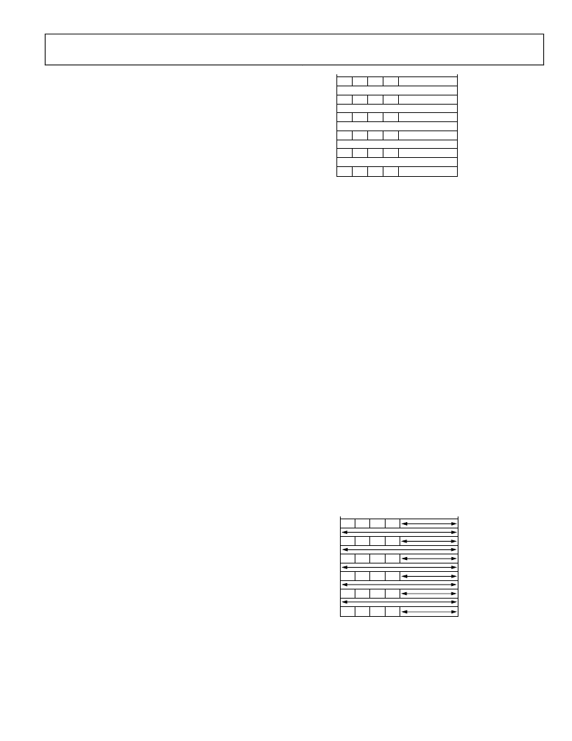
0
Figure 34. Typical DMA External Memory Preconfiguration
4.
The DMA is initiated by writing to the ADC SFRs in the
following sequence:
a.
ADCCON2 is written to enable the DMA mode, i.e.,
MOV ADCCON2, #40H; DMA mode enabled.
b.
ADCCON1 is written to configure the conversion
time and power-up of the ADC. It can also enable
Timer 2 driven conversions or external triggered
conversions if required.
c.
ADC conversions are initiated. This is done by starting
single conversions, starting Timer 2, running for
Timer 2 conversions, or receiving an external trigger.
When the DMA conversions are complete, the ADC interrupt
bit, ADCI, is set by hardware, and the external SRAM contains
the new ADC conversion results as shown in Figure 35. Note
that no result is written to the last two memory locations.
When the DMA mode logic is active, it takes the responsibility
of storing the ADC results away from both the user and the core
logic of the part. As the DMA interface writes the results of the
ADC conversions to external memory, it takes over the external
memory interface from the core. Thus, any core instructions
that access the external memory while DMA mode is enabled
does not get access to the external memory. The core executes
the instructions, and they take the same time to execute, but
they cannot access the external memory.
1
1
1
1
0
0
1
1
0
0
1
1
1
0
0
0
0
1
0
1
0
0
1
0
00000AH
000000H
CONVERSION RESULT
FOR ADC CH 2
CONVERSION RESULT
FOR ADC CH 5
CONVERSION RESULT
FOR ADC CH 3
CONVERSION RESULT
FOR TEMP SENSOR
STOP COMMAND
NO CONVERSION
RESULT WRITTEN HERE
0
Figure 35. Typical External Memory Configuration Post ADC DMA Operation
相關PDF資料 |
PDF描述 |
|---|---|
| ADUC843BCP32-3 | MicroConverter 12-Bit ADCs and DACs with Embedded High Speed 62-kB Flash MCU |
| ADUC842BCP32-5 | MicroConverter 12-Bit ADCs and DACs with Embedded High Speed 62-kB Flash MCU |
| ADUC843BCP32-5 | MicroConverter 12-Bit ADCs and DACs with Embedded High Speed 62-kB Flash MCU |
| ADUC842BCP8-3 | MicroConverter 12-Bit ADCs and DACs with Embedded High Speed 62-kB Flash MCU |
| ADUC843BCP8-3 | MicroConverter 12-Bit ADCs and DACs with Embedded High Speed 62-kB Flash MCU |
相關代理商/技術參數 |
參數描述 |
|---|---|
| ADUC842BCP32-5 | 制造商:Analog Devices 功能描述:MCU 8-Bit ADuC8xx 8052 CISC 62KB Flash 5V 56-Pin LFCSP EP |
| ADUC842BCP62-3 | 制造商:Analog Devices 功能描述:MCU 8-bit ADuC8xx 8052 CISC 62KB Flash 3V 56-Pin LFCSP EP |
| ADUC842BCP62-3U | 制造商:Analog Devices 功能描述:MICROCONVERTER 1-CYCLE VERSION ADUC833 - Trays |
| ADUC842BCP62-3-U2 | 制造商:Analog Devices 功能描述:MICROCONVERTER 1-CYCLE VERSION ADUC834 - Trays |
| ADUC842BCP62-5 | 制造商:Rochester Electronics LLC 功能描述: 制造商:Analog Devices 功能描述: |
發布緊急采購,3分鐘左右您將得到回復。