- 您現在的位置:買賣IC網 > PDF目錄374039 > ADUC842BCP32-3 (ANALOG DEVICES INC) MicroConverter 12-Bit ADCs and DACs with Embedded High Speed 62-kB Flash MCU PDF資料下載
參數資料
| 型號: | ADUC842BCP32-3 |
| 廠商: | ANALOG DEVICES INC |
| 元件分類: | 微控制器/微處理器 |
| 英文描述: | MicroConverter 12-Bit ADCs and DACs with Embedded High Speed 62-kB Flash MCU |
| 中文描述: | 8-BIT, FLASH, 8.38 MHz, MICROCONTROLLER, QCC56 |
| 封裝: | 8 X 8 MM, LEAD FRAME, MO-220VLLD2, CSP-56 |
| 文件頁數: | 40/88頁 |
| 文件大小: | 903K |
| 代理商: | ADUC842BCP32-3 |
第1頁第2頁第3頁第4頁第5頁第6頁第7頁第8頁第9頁第10頁第11頁第12頁第13頁第14頁第15頁第16頁第17頁第18頁第19頁第20頁第21頁第22頁第23頁第24頁第25頁第26頁第27頁第28頁第29頁第30頁第31頁第32頁第33頁第34頁第35頁第36頁第37頁第38頁第39頁當前第40頁第41頁第42頁第43頁第44頁第45頁第46頁第47頁第48頁第49頁第50頁第51頁第52頁第53頁第54頁第55頁第56頁第57頁第58頁第59頁第60頁第61頁第62頁第63頁第64頁第65頁第66頁第67頁第68頁第69頁第70頁第71頁第72頁第73頁第74頁第75頁第76頁第77頁第78頁第79頁第80頁第81頁第82頁第83頁第84頁第85頁第86頁第87頁第88頁
ADuC841/ADuC842/ADuC843
The endpoint nonlinearities illustrated in Figure 43 become
worse as a function of output loading. Most of the part’s
specifications assume a 10 k resistive load to ground at the
DAC output. As the output is forced to source or sink more
current, the nonlinear regions at the top or bottom (respectively)
of Figure 43 become larger. Larger current demands can sig-
nificantly limit output voltage swing. Figure 44 and Figure 45
illustrate this behavior. Note that the upper trace in each of
these figures is valid only for an output range selection of
0 V-to-AV
DD
. In 0 V-to-V
REF
mode, DAC loading does not cause
high-side voltage drops as long as the reference voltage remains
below the upper trace in the corresponding figure. For example,
if AV
DD
= 3 V and V
REF
= 2.5 V, the high-side voltage is not be
affected by loads less than 5 mA. But somewhere around 7 mA,
the upper curve in Figure 45 drops below 2.5 V (V
REF
), indicating
that at these higher currents the output is not capable of
reaching V
REF
.
Rev. 0 | Page 40 of 88
To reduce the effects of the saturation of the output amplifier at
values close to ground and to give reduced offset and gain errors,
the internal buffer can be bypassed. This is done by setting the
DBUF bit in the CFG841/CFG842 register. This allows a full
rail-to-rail output from the DAC, which should then be buffered
externally using a dual-supply op amp in order to get a rail-to-
rail output. This external buffer should be located as close as
physically possible to the DAC output pin on the PCB. Note that
the unbuffered mode works only in the 0 V to V
REF
range.
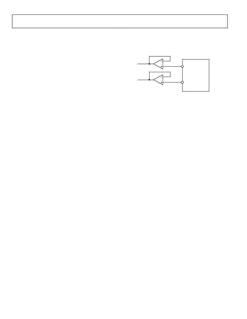
To drive significant loads with the DAC outputs, external
buffering may be required (even with the internal buffer
enabled), as illustrated in Figure 46
.
Table 11 lists some
recommended op amps.
ADuC841/
ADuC842
DAC0
DAC1
0
Figure 46. Buffering the DAC Outputs
The DAC output buffer also features a high impedance disable
function. In the chip’s default power-on state, both DACs are
disabled, and their outputs are in a high impedance state (or
three-state) where they remain inactive until enabled in
software. This means that if a zero output is desired during
power-up or power-down transient conditions, then a pull-
down resistor must be added to each DAC output. Assuming
this resistor is in place, the DAC outputs remain at ground
potential whenever the DAC is disabled.
相關PDF資料 |
PDF描述 |
|---|---|
| ADUC843BCP32-3 | MicroConverter 12-Bit ADCs and DACs with Embedded High Speed 62-kB Flash MCU |
| ADUC842BCP32-5 | MicroConverter 12-Bit ADCs and DACs with Embedded High Speed 62-kB Flash MCU |
| ADUC843BCP32-5 | MicroConverter 12-Bit ADCs and DACs with Embedded High Speed 62-kB Flash MCU |
| ADUC842BCP8-3 | MicroConverter 12-Bit ADCs and DACs with Embedded High Speed 62-kB Flash MCU |
| ADUC843BCP8-3 | MicroConverter 12-Bit ADCs and DACs with Embedded High Speed 62-kB Flash MCU |
相關代理商/技術參數 |
參數描述 |
|---|---|
| ADUC842BCP32-5 | 制造商:Analog Devices 功能描述:MCU 8-Bit ADuC8xx 8052 CISC 62KB Flash 5V 56-Pin LFCSP EP |
| ADUC842BCP62-3 | 制造商:Analog Devices 功能描述:MCU 8-bit ADuC8xx 8052 CISC 62KB Flash 3V 56-Pin LFCSP EP |
| ADUC842BCP62-3U | 制造商:Analog Devices 功能描述:MICROCONVERTER 1-CYCLE VERSION ADUC833 - Trays |
| ADUC842BCP62-3-U2 | 制造商:Analog Devices 功能描述:MICROCONVERTER 1-CYCLE VERSION ADUC834 - Trays |
| ADUC842BCP62-5 | 制造商:Rochester Electronics LLC 功能描述: 制造商:Analog Devices 功能描述: |
發布緊急采購,3分鐘左右您將得到回復。