- 您現在的位置:買賣IC網 > PDF目錄379831 > CDC9842 (Texas Instruments, Inc.) PC Motherboard Clock Sythesizer/Drivers with 3 - State Outputs(PC母板時鐘合成器/驅動器(三態輸出)) PDF資料下載
參數資料
| 型號: | CDC9842 |
| 廠商: | Texas Instruments, Inc. |
| 英文描述: | PC Motherboard Clock Sythesizer/Drivers with 3 - State Outputs(PC母板時鐘合成器/驅動器(三態輸出)) |
| 中文描述: | 電腦主板時鐘Sythesizer / 3驅動器-態輸出(電腦母板時鐘合成器/驅動器(三態輸出)) |
| 文件頁數: | 1/7頁 |
| 文件大小: | 132K |
| 代理商: | CDC9842 |
CDC9842
PC MOTHERBOARD CLOCK SYNTHESIZER/DRIVER
WITH 3-STATE OUTPUTS
SCAS546B – NOVEMBER 1995 – REVISED MAY 1996
1
POST OFFICE BOX 655303
DALLAS, TEXAS 75265
Provides System Clock Solution for
Pentium
/82430X/82430VX and
PentiumPro 82440FX Chipsets
Four Host-Clock Outputs With
Programmable Frequency (50 MHz, 60 MHz
and 66 MHz)
Six PCI Clock Outputs at Half-CPU
Frequency
One 48-MHz Universal Serial Bus (USB)
Clock Output
Three 14.318-MHz Reference Clock Outputs
All Output Clock Frequencies Derived From
a Single 14.31818-MHz Crystal Input
LVTTL-Compatible Inputs and Outputs
Internal Loop Filters for Phase-Locked
Loops Eliminate the Need for External
Components
Operates at 3.3 V
CC
Packaged in Plastic Small-Outline Package
description
The CDC9842 is a high-performance clock synthesizer/driver that generates the system clocks necessary to
support Pentium
/82430X/82430VX and PentiumPro 82440FX chipsets. Four host-clock outputs (HCLKn) are
programmable to one of three frequencies (50 MHz, 60 MHz, or 66 MHz) via the SEL0 and SEL1 control inputs.
Six PCI-clock outputs (PCLKn) are half the frequency of CPU clock outputs and are delayed 1 ns to 4 ns from
the rising edge of the CPU clock. In addition, a universal serial bus (USB) clock output at 48 MHz (SBCLK) and
three 14.318-MHz reference clock outputs (REF0, REF1, REF2) are provided.
All output frequencies are generated from a 14.318-MHZ crystal input. A reference clock can be provided at the
X1 input instead of a crystal input.
Two phase-locked loops (PLLs) are used to generate the host clock frequency and the 48-MHz clock frequency.
On-chip loop filters and internal feedback eliminate the need for external components. The PCI-clock
frequency is derived directly from the host-clock frequency. The PLL circuit can be bypassed in the TEST mode
(i.e., SEL0 = SEL1 = H) to distribute a test clock provided at the X1 input.
The host- and PCI-clock outputs provide low-skew/low-jitter clock signals for reliable clock operation. All outputs
are 3 state and are enabled via OE.
Because the CDC9842 is based on PLL circuitry, it requires a stabilization time to achieve phase-lock of the PLL.
This stabilization time is required following power up and application of a fixed-frequency, fixed-phase signal
at the X1 input, as well as following any changes to the OE or SELn inputs.
Copyright
1996, Texas Instruments Incorporated
PRODUCTION DATA information is current as of publication date.
Products conform to specifications per the terms of Texas Instruments
standard warranty. Production processing does not necessarily include
testing of all parameters.
Pentium is a trademark of Intel Corporation.
Please be aware that an important notice concerning availability, standard warranty, and use in critical applications of
Texas Instruments semiconductor products and disclaimers thereto appears at the end of this data sheet.
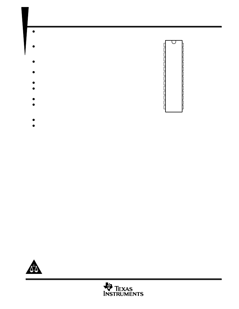
1
2
3
4
5
6
7
8
9
10
11
12
13
14
28
27
26
25
24
23
22
21
20
19
18
17
16
15
V
CC
X1
X2
GND
OE
HCLK0
HCLK1
V
CC
HCLK2
HCLK3
GND
SEL1
SEL0
V
CC
REF0
REF1
V
CC
REF2
SBCLK
GND
PCLK0
PCLK1
V
CC
PCLK2
PCLK3
GND
PCLK4
PCLK5
DW PACKAGE
(TOP VIEW)
相關PDF資料 |
PDF描述 |
|---|---|
| CDC9843 | PC MOTHERBOARD CLOCK SYNTHESIZER/DRIVER WITH 3-STATE OUTPUTS |
| CDC9843DW | PC MOTHERBOARD CLOCK SYNTHESIZER/DRIVER WITH 3-STATE OUTPUTS |
| CDC9843DWR | PC MOTHERBOARD CLOCK SYNTHESIZER/DRIVER WITH 3-STATE OUTPUTS |
| CDCD5704_07 | Rambus XDR CLOCK GENERATOR |
| CDCDLP223_07 | 3.3 V Clock Synthesizer for DLP Systems |
相關代理商/技術參數 |
參數描述 |
|---|---|
| CDC9842DW | 制造商:Rochester Electronics LLC 功能描述:- Bulk |
| CDC9842DWR | 制造商:Rochester Electronics LLC 功能描述:- Bulk |
| CDC9843 | 制造商:TI 制造商全稱:Texas Instruments 功能描述:PC MOTHERBOARD CLOCK SYNTHESIZER/DRIVER WITH 3-STATE OUTPUTS |
| CDC9843DW | 制造商:Rochester Electronics LLC 功能描述:- Bulk |
| CDC9843DWR | 制造商:Texas Instruments 功能描述:CPU SYSTEM CLOCK GENERATOR, 28 Pin, Plastic, SOP |
發布緊急采購,3分鐘左右您將得到回復。