- 您現在的位置:買賣IC網 > PDF目錄375763 > FDA20N50_07 (Fairchild Semiconductor Corporation) 500V N-Channel MOSFET PDF資料下載
參數資料
| 型號: | FDA20N50_07 |
| 廠商: | Fairchild Semiconductor Corporation |
| 英文描述: | 500V N-Channel MOSFET |
| 中文描述: | 500V N溝道MOSFET |
| 文件頁數: | 2/9頁 |
| 文件大小: | 324K |
| 代理商: | FDA20N50_07 |
2
www.fairchildsemi.com
FDA20N50 Rev. B
F
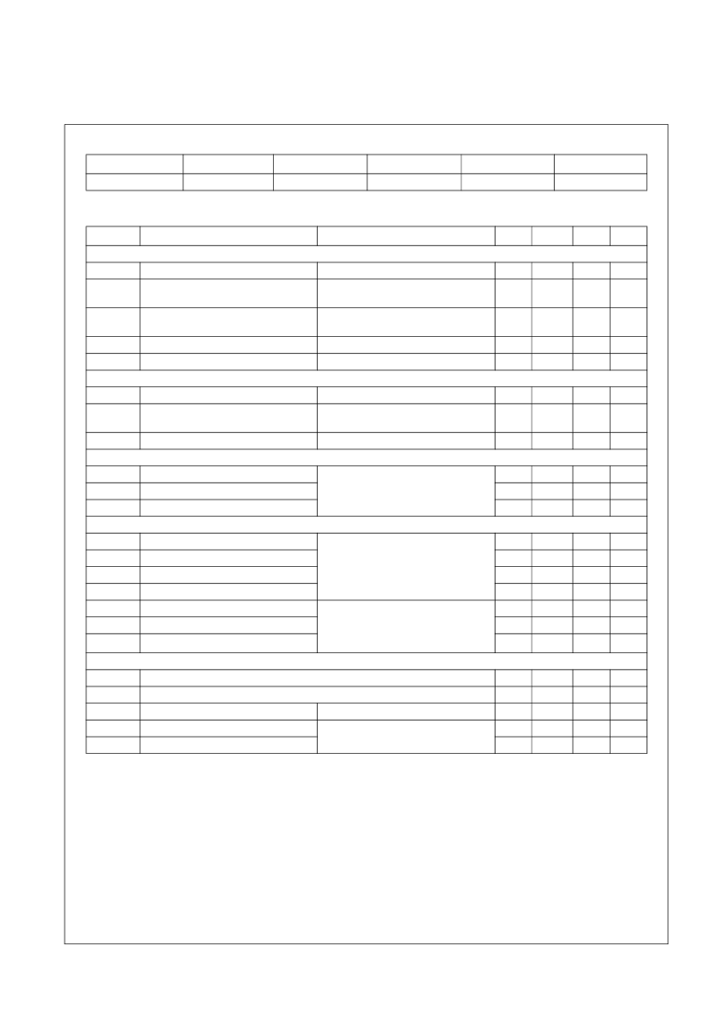
Package Marking and Ordering Information
Electrical Characteristics
T
C
= 25°C unless otherwise noted
NOTES:
1. Repetitive Rating: Pulse width limited by maximum junction temperature
2. L = 4.1mH, I
AS
= 22A, V
DD
= 50V, R
G
= 25
Ω
, Starting T
J
= 25
°
C
3. I
SD
≤
22A, di/dt
≤
200A/
μ
s, V
DD
≤
BV
DSS
, Starting T
J
= 25
°
C
4. Pulse Test: Pulse width
≤
300
μ
s, Duty Cycle
≤
2%
5. Essentially Independent of Operating Temperature Typical Characteristics
Device Marking
Device
Package
Reel Size
Tape Width
Quantity
FDA20N50
FDA20N50
TO-3P
--
--
30
Symbol
Parameter
Conditions
Min
Typ
Max
Units
Off Characteristics
BV
DSS
Δ
BV
DSS
/
Δ
T
J
I
DSS
Drain-Source Breakdown Voltage
V
GS
= 0V, I
D
= 250
μ
A, T
J
= 25
°
C
500
--
--
V
Breakdown Voltage Temperature
Coefficient
I
D
= 250
μ
A, Referenced to 25
°
C
--
0.50
--
V/
°
C
Zero Gate Voltage Drain Current
V
DS
= 500V, V
GS
= 0V
V
DS
= 400V, T
C
= 125
°
C
V
GS
= 30V, V
DS
= 0V
V
GS
= -30V, V
DS
= 0V
--
--
--
--
1
10
μ
A
μ
A
I
GSSF
I
GSSR
On Characteristics
Gate-Body Leakage Current, Forward
--
--
100
nA
Gate-Body Leakage Current, Reverse
--
--
-100
nA
V
GS(th)
R
DS(on)
Gate Threshold Voltage
V
DS
= V
GS
, I
D
= 250
μ
A
3.0
--
5.0
V
Static Drain-Source
On-Resistance
V
GS
= 10V, I
D
= 11A
--
0.20
0.23
Ω
g
FS
Dynamic Characteristics
Forward Transconductance
V
DS
= 40V, I
D
= 11A
(Note 4)
--
24.6
--
S
C
iss
C
oss
C
rss
Switching Characteristics
Input Capacitance
V
DS
= 25V, V
GS
= 0V,
f = 1.0MHz
--
2400
3120
pF
Output Capacitance
--
355
465
pF
Reverse Transfer Capacitance
--
27
--
pF
t
d(on)
t
r
t
d(off)
t
f
Q
g
Q
gs
Q
gd
Turn-On Delay Time
V
DD
= 250V, I
D
= 20A
R
G
= 25
Ω
(Note 4, 5)
--
95
200
ns
Turn-On Rise Time
--
375
760
ns
Turn-Off Delay Time
--
100
210
ns
Turn-Off Fall Time
--
105
220
ns
Total Gate Charge
V
DS
= 400V, I
D
= 20A
V
GS
= 10V
(Note 4, 5)
--
45.6
59.5
nC
Gate-Source Charge
--
14.8
--
nC
Gate-Drain Charge
--
21.6
--
nC
Drain-Source Diode Characteristics and Maximum Ratings
I
S
I
SM
V
SD
t
rr
Q
rr
Maximum Continuous Drain-Source Diode Forward Current
--
--
20
A
Maximum Pulsed Drain-Source Diode Forward Current
--
--
80
A
Drain-Source Diode Forward Voltage
V
GS
= 0V, I
S
= 22A
V
GS
= 0V, I
S
= 20A
dI
F
/dt =100A/
μ
s
(Note 4)
--
--
1.4
V
Reverse Recovery Time
--
507
--
ns
Reverse Recovery Charge
--
7.20
--
μ
C
相關PDF資料 |
PDF描述 |
|---|---|
| FDA2712 | N-Channel UltraFET Trench MOSFET 250V, 64A, 34mヘ |
| FDA33N25 | N-Channel MOSFET |
| FDA50N50 | 500V N-Channel MOSFET |
| FDH50N50 | 500V N-Channel MOSFET |
| FDA59N25 | 250V N-Channel MOSFET |
相關代理商/技術參數 |
參數描述 |
|---|---|
| FDA20N50F | 功能描述:MOSFET 500V N-Channel RoHS:否 制造商:STMicroelectronics 晶體管極性:N-Channel 汲極/源極擊穿電壓:650 V 閘/源擊穿電壓:25 V 漏極連續電流:130 A 電阻汲極/源極 RDS(導通):0.014 Ohms 配置:Single 最大工作溫度: 安裝風格:Through Hole 封裝 / 箱體:Max247 封裝:Tube |
| FDA20N50F_12 | 制造商:FAIRCHILD 制造商全稱:Fairchild Semiconductor 功能描述:N-Channel MOSFET 500V, 22A, 0.26?? |
| FDA210 | 制造商:未知廠家 制造商全稱:未知廠家 功能描述:PHOTOVOLTAIC-OUTPUT OPTOCOUPLER |
| FDA210E | 制造商:未知廠家 制造商全稱:未知廠家 功能描述:PHOTOVOLTAIC-OUTPUT OPTOCOUPLER |
| FDA210ES | 制造商:未知廠家 制造商全稱:未知廠家 功能描述:PHOTOVOLTAIC-OUTPUT OPTOCOUPLER |
發布緊急采購,3分鐘左右您將得到回復。