- 您現在的位置:買賣IC網 > PDF目錄375763 > FDA33N25 (FAIRCHILD SEMICONDUCTOR CORP) N-Channel MOSFET PDF資料下載
參數資料
| 型號: | FDA33N25 |
| 廠商: | FAIRCHILD SEMICONDUCTOR CORP |
| 元件分類: | JFETs |
| 英文描述: | N-Channel MOSFET |
| 中文描述: | 33 A, 250 V, 0.094 ohm, N-CHANNEL, Si, POWER, MOSFET |
| 封裝: | ROHS COMPLIANT, TO-3PN, 3 PIN |
| 文件頁數: | 2/8頁 |
| 文件大小: | 607K |
| 代理商: | FDA33N25 |
F
FDA33N25 Rev. A
www.fairchildsemi.com
2
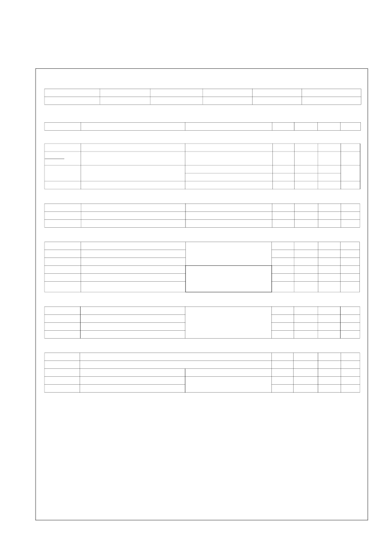
Package Marking and Ordering Information
Electrical Characteristics
T
C
= 25
o
C unless otherwise noted
Off Characteristics
On Characteristics
Dynamic Characteristics
Switching Characteristics
Drain-Source Diode Characteristics
Device Marking
FDA33N25
Device
FDA33N25
Package
TO-3PN
Reel Size
-
Tape Width
-
Quantity
50
Symbol
Parameter
Test Conditions
Min.
Typ.
Max.
Units
BV
DSS
BV
DSS
T
J
Drain to Source Breakdown Voltage
Breakdown Voltage Temperature
Coefficient
I
D
= 250
μ
A, V
GS
= 0V, T
J
= 25
o
C
250
-
-
V
I
D
= 250
μ
A, Referenced to 25
o
C
-
0.34
-
V/
o
C
I
DSS
Zero Gate Voltage Drain Current
V
DS
= 250V, V
GS
= 0V
V
DS
= 200V, T
C
= 125
o
C
V
GS
= ±30V, V
DS
= 0V
-
-
-
-
-
-
1
μ
A
10
±100
I
GSS
Gate to Body Leakage Current
nA
V
GS(th)
R
DS(on)
g
FS
Gate Threshold Voltage
Static Drain to Source On Resistance
Forward Transconductance
V
GS
= V
DS
, I
D
= 250
μ
A
V
GS
= 10V, I
D
= 16.5A
V
DS
= 20V, I
D
= 16.5A
(Note 4)
3.0
-
-
-
5.0
0.094
-
V
S
0.088
24.2
C
iss
C
oss
C
rss
Q
g(tot)
Q
gs
Q
gd
Input Capacitance
Output Capacitance
Reverse Transfer Capacitance
Total Gate Charge at 10V
Gate to Source Gate Charge
V
DS
= 25V, V
GS
= 0V
f = 1MHz
-
-
-
-
-
1655
315
35
36
10.8
2200
420
55
46.8
-
pF
pF
pF
nC
nC
V
DS
= 200V, I
D
= 33A
V
GS
= 10V
(Note 4, 5)
Gate to Drain “Miller” Charge
-
16
-
nC
t
d(on)
t
r
t
d(off)
t
f
Turn-On Delay Time
Turn-On Rise Time
Turn-Off Delay Time
Turn-Off Fall Time
V
DD
= 125V, I
D
= 33A
R
G
= 25
(Note 4, 5)
-
-
-
-
33
142
77
68
76
293
165
146
ns
ns
ns
ns
I
S
I
SM
V
SD
t
rr
Q
rr
Notes:
1. Repetitive Rating: Pulse width limited by maximum junction temperature
2. L = 1.35mH, I
AS
= 33A, V
DD
= 50V, R
G
= 25
, Starting T
J
= 25
°
C
3. I
SD
≤
33A, di/dt
≤
200A/
μ
s, V
DD
≤
BV
DSS
, Starting T
J
= 25
°
C
4. Pulse Test: Pulse width
≤
300
μ
s, Duty Cycle
≤
2%
Maximum Continuous Drain to Source Diode Forward Current
Maximum Pulsed Drain to Source Diode Forward Current
Drain to Source Diode Forward Voltage
Reverse Recovery Time
Reverse Recovery Charge
-
-
-
-
-
-
-
-
33
132
1.4
-
-
A
A
V
ns
μ
C
V
GS
= 0V, I
SD
= 33A
V
GS
= 0V, I
SD
= 33A
dI
F
/dt = 100A/
μ
s
(Note 4)
256
2.3
5. Essentially Independent of Operating Temperature Typical Characteristics
相關PDF資料 |
PDF描述 |
|---|---|
| FDA50N50 | 500V N-Channel MOSFET |
| FDH50N50 | 500V N-Channel MOSFET |
| FDA59N25 | 250V N-Channel MOSFET |
| FDA59N30 | 300V N-Channel MOSFET |
| FDA62N28 | 280V N-Channel MOSFET |
相關代理商/技術參數 |
參數描述 |
|---|---|
| FDA-37PF | 制造商:HRS 制造商全稱:HRS 功能描述:FD TYPE CONNECTOR FOR RIBBON CABLE |
| FDA-37SF | 制造商:HRS 制造商全稱:HRS 功能描述:FD TYPE CONNECTOR FOR RIBBON CABLE |
| FDA38N30 | 功能描述:MOSFET UniFET1 300V N-chan MOSFET RoHS:否 制造商:STMicroelectronics 晶體管極性:N-Channel 汲極/源極擊穿電壓:650 V 閘/源擊穿電壓:25 V 漏極連續電流:130 A 電阻汲極/源極 RDS(導通):0.014 Ohms 配置:Single 最大工作溫度: 安裝風格:Through Hole 封裝 / 箱體:Max247 封裝:Tube |
| FDA4100LV | 制造商:STMicroelectronics 功能描述:ABD AUDIO & POWER - Trays |
| F-DA50A | 制造商:Cosel Usa Inc 功能描述:POWER SUPPLY; DAS SERIES HEAT SINK 制造商:Cosel Usa Inc 功能描述:Optional Accessories, OP Series |
發布緊急采購,3分鐘左右您將得到回復。