- 您現在的位置:買賣IC網 > PDF目錄375777 > FDN335 (Fairchild Semiconductor Corporation) N-Channel 2.5V Specified PowerTrenchTM MOSFET PDF資料下載
參數資料
| 型號: | FDN335 |
| 廠商: | Fairchild Semiconductor Corporation |
| 英文描述: | N-Channel 2.5V Specified PowerTrenchTM MOSFET |
| 中文描述: | N溝道MOSFET的2.5V的指定PowerTrenchTM |
| 文件頁數: | 2/8頁 |
| 文件大小: | 210K |
| 代理商: | FDN335 |
F
FDN335N Rev. C
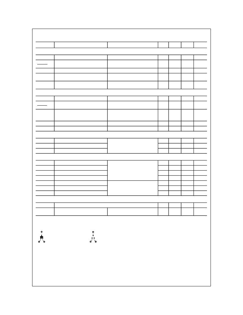
Electrical Characteristics
T
A
= 25°C unless otherwise noted
Symbol
Parameter
Test Conditions
Min
Typ
Max
Units
Off Characteristics
BV
DSS
BV
DSS
T
J
I
DSS
I
GSSF
Drain-Source Breakdown Voltage
Breakdown Voltage Temperature
Coefficient
Zero Gate Voltage Drain Current
Gate-Body Leakage Current,
Forward
Gate-Body Leakage Current,
Reverse
V
GS
= 0 V, I
D
= 250
μ
A
I
D
= 250
μ
A,Referenced to 25
°
C
20
V
14
mV/
°
C
V
DS
= 16 V, V
GS
= 0 V
V
GS
= 8 V, V
DS
= 0 V
1
μ
A
nA
100
I
GSSR
V
GS
= -8 V, V
DS
= 0 V
-100
nA
On Characteristics
(Note 2)
V
GS(th)
Gate Threshold Voltage
V
GS(th)
T
J
Temperature Coefficient
R
DS(ON)
Static Drain-Source
On-Resistance
V
DS
= V
GS
, I
D
= 250
μ
A
I
D
= 250
μ
A,Referenced to 25
°
C
0.4
0.9
-3
1.5
V
Gate Threshold Voltage
mV/
°
C
V
GS
= 4.5 V, I
D
= 1.7 A
V
GS
= 4.5 V, I
D
= 1.7 A,T
J
= 125
°
C
V
GS
= 2.5 V, I
D
= 1.5 A
V
GS
= 4.5 V, V
DS
= 5 V
V
DS
= 5 V, I
D
= 1.5 A
0.055
0.079
0.078
0.070
0.120
0.100
I
D(on)
g
FS
On-State Drain Current
Forward Transconductance
8
A
S
7
Dynamic Characteristics
C
iss
Input Capacitance
C
oss
Output Capacitance
C
rss
Reverse Transfer Capacitance
310
80
40
pF
pF
pF
V
DS
= 10 V, V
GS
= 0 V,
f = 1.0 MHz
Switching Characteristics
(Note 2)
t
d(on)
Turn-On Delay Time
t
r
Turn-On Rise Time
t
d(off)
Turn-Off Delay Time
t
f
Turn-Off Fall Time
Q
g
Total Gate Charge
Q
gs
Gate-Source Charge
Q
gd
Gate-Drain Charge
5
15
17
20
10
5
ns
ns
ns
ns
nC
nC
nC
8.5
11
3
3.5
0.55
0.95
V
DD
= 10 V, I
D
= 1 A,
V
GS
= 4.5 V, R
GEN
= 6
V
DS
= 10 V, I
D
= 1.7 A,
V
GS
= 4.5 V,
Drain-Source Diode Characteristics and Maximum Ratings
I
S
Maximum Continuous Drain-Source Diode Forward Current
V
SD
Drain-Source Diode Forward
Voltage
0.42
1.2
A
V
V
GS
= 0 V, I
S
= 0.42 A
(Note 2)
0.7
Notes:
1:
R
is the sum of the junction-to-case and case-to-ambient thermal resistance where the case thermal reference is defined as the solder mounting
surface of the drain pins. R
θ
JC
is guaranteed by design while R
θ
CA
is determined by the user's board design.
Scale 1 : 1 on letter size paper
2:
Pulse Test: Pulse Width
≤
300
μ
s, Duty Cycle
≤
2.0%
a) 250
°
C/W when
mounted on a 0.02 in
2
Pad of 2 oz. Cu.
b) 270
°
C/W when mounted
on a minimum pad.
相關PDF資料 |
PDF描述 |
|---|---|
| FDN335N | N-Channel 2.5V Specified PowerTrenchTM MOSFET |
| FDN336 | Single P-Channel 2.5V Specified PowerTrenchTM MOSFET |
| FDN336P | Single P-Channel 2.5V Specified PowerTrenchTM MOSFET |
| FDN337N | N-Channel Logic Level Enhancement Mode Field Effect Transistor |
| FDN338 | P-Channel Logic Level Enhancement Mode Field Effect Transistor |
相關代理商/技術參數 |
參數描述 |
|---|---|
| FDN335N | 功能描述:MOSFET SSOT-3 N-CH 20V RoHS:否 制造商:STMicroelectronics 晶體管極性:N-Channel 汲極/源極擊穿電壓:650 V 閘/源擊穿電壓:25 V 漏極連續電流:130 A 電阻汲極/源極 RDS(導通):0.014 Ohms 配置:Single 最大工作溫度: 安裝風格:Through Hole 封裝 / 箱體:Max247 封裝:Tube |
| FDN335N | 制造商:Fairchild Semiconductor Corporation 功能描述:MOSFET N SOT-23 |
| FDN335N_NL | 功能描述:MOSFET N-CH 20V RoHS:否 制造商:STMicroelectronics 晶體管極性:N-Channel 汲極/源極擊穿電壓:650 V 閘/源擊穿電壓:25 V 漏極連續電流:130 A 電阻汲極/源極 RDS(導通):0.014 Ohms 配置:Single 最大工作溫度: 安裝風格:Through Hole 封裝 / 箱體:Max247 封裝:Tube |
| FDN335N_Q | 功能描述:MOSFET SSOT-3 N-CH 20V RoHS:否 制造商:STMicroelectronics 晶體管極性:N-Channel 汲極/源極擊穿電壓:650 V 閘/源擊穿電壓:25 V 漏極連續電流:130 A 電阻汲極/源極 RDS(導通):0.014 Ohms 配置:Single 最大工作溫度: 安裝風格:Through Hole 封裝 / 箱體:Max247 封裝:Tube |
| FDN335N-CUT TAPE | 制造商:FAIRCHILD 功能描述:FDN335N Series 20 V 0.07 Ohm N-Channel 2.5V Specified PowerTrench Mosfet SSOT-3 |
發布緊急采購,3分鐘左右您將得到回復。