- 您現(xiàn)在的位置:買賣IC網(wǎng) > PDF目錄385323 > GS832418C-225I (GSI TECHNOLOGY) 2M x 18, 1M x 36, 512K x 72 36Mb S/DCD Sync Burst SRAMs PDF資料下載
參數(shù)資料
| 型號: | GS832418C-225I |
| 廠商: | GSI TECHNOLOGY |
| 元件分類: | DRAM |
| 英文描述: | 2M x 18, 1M x 36, 512K x 72 36Mb S/DCD Sync Burst SRAMs |
| 中文描述: | 2M X 18 CACHE SRAM, 6 ns, PBGA209 |
| 封裝: | 14 X 22 MM, 1 MM PITCH, BGA-209 |
| 文件頁數(shù): | 34/46頁 |
| 文件大小: | 1149K |
| 代理商: | GS832418C-225I |
第1頁第2頁第3頁第4頁第5頁第6頁第7頁第8頁第9頁第10頁第11頁第12頁第13頁第14頁第15頁第16頁第17頁第18頁第19頁第20頁第21頁第22頁第23頁第24頁第25頁第26頁第27頁第28頁第29頁第30頁第31頁第32頁第33頁當(dāng)前第34頁第35頁第36頁第37頁第38頁第39頁第40頁第41頁第42頁第43頁第44頁第45頁第46頁
Rev: 1.00 10/2001
Specifications cited are subject to change without notice. For latest documentation see http://www.gsitechnology.com.
34/46
2001, Giga Semiconductor, Inc.
Preliminary
GS832418(B/C)/GS832436(B/C)/GS832472(C)
Capture-DR state and then is placed between the TDI and TDO pins when the controller is moved to Shift-DR state. SAMPLE-Z,
SAMPLE/PRELOAD and EXTEST instructions can be used to activate the Boundary Scan Register.
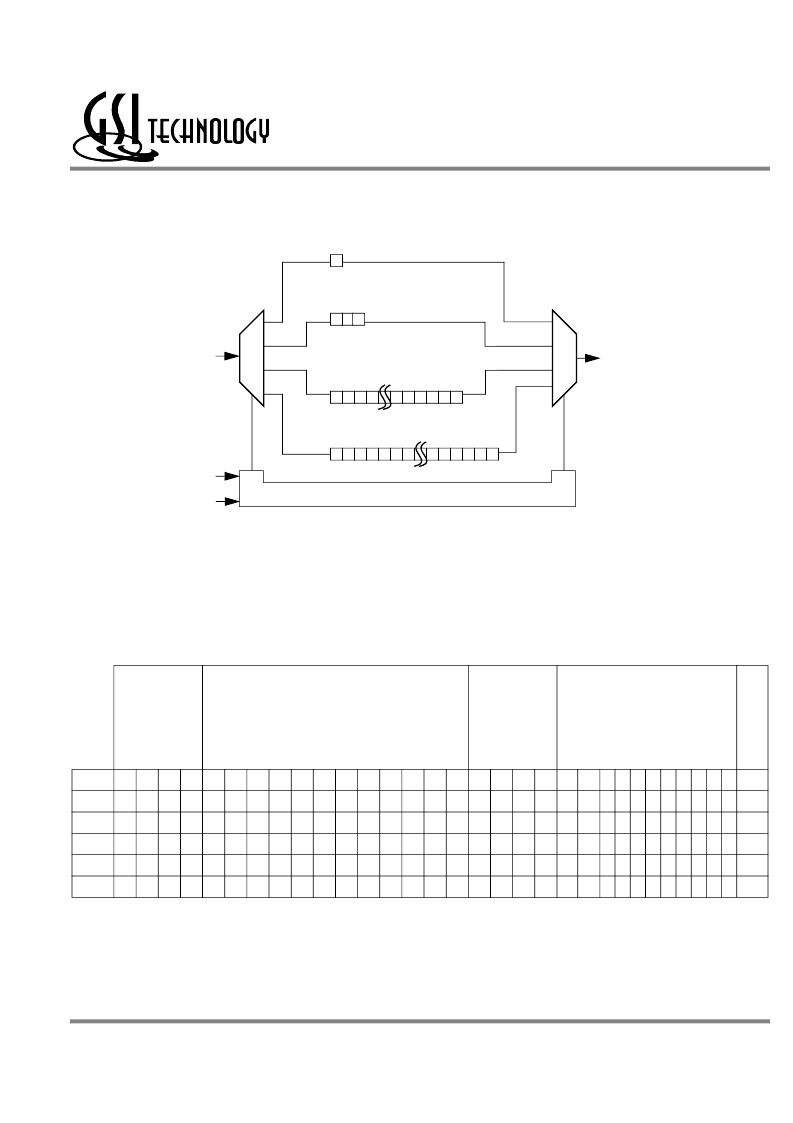
JTAG TAP Block Diagram
Identification (ID) Register
The ID Register is a 32-bit register that is loaded with a device and vendor specific 32-bit code when the controller is put in
Capture-DR state with the IDCODE command loaded in the Instruction Register. The code is loaded from a 32-bit on-chip ROM.
It describes various attributes of the RAM as indicated below. The register is then placed between the TDI and TDO pins when the
controller is moved into Shift-DR state. Bit 0 in the register is the LSB and the first to reach TDO when shifting begins.
Tap Controller Instruction Set
Overview
There are two classes of instructions defined in the Standard 1149.1-1990; the standard (Public) instructions, and device specific
(Private) instructions. Some Public instructions are mandatory for 1149.1 compliance. Optional Public instructions must be
ID Register Contents
Die
Revision
Code
Not Used
I/O
Configuration
GSI Technology
JEDEC Vendor
ID Code
P
0
1
1
1
1
1
Bit #
x72
x36
x32
x18
x16
31 30 29 28 27 26 25 24 23 22 21 20 19 18 17 16 15 14 13 12 11 10 9 8 7 6 5 4 3 2 1
X
X
X
X
0
0
0
0
0
0
0
0
0
0
X
X
X
X
0
0
0
0
0
0
0
0
0
0
X
X
X
X
0
0
0
0
0
0
0
0
0
0
X
X
X
X
0
0
0
0
0
0
0
0
0
0
X
X
X
X
0
0
0
0
0
0
0
0
0
0
0
0
0
0
0
0
0
0
0
0
1
1
1
1
1
0
0
1
0
1
0
0
0
1
1
1
0
0
0
0
0
0
0
0
0
0
0
0
0
0
0 1 1 0 1 1 0 0 1
0 1 1 0 1 1 0 0 1
0 1 1 0 1 1 0 0 1
0 1 1 0 1 1 0 0 1
0 1 1 0 1 1 0 0 1
Instruction Register
ID Code Register
·
31 30 29
Boundary Scan Register
· · ·
· · ·
n
0
1
2
0
1
2
· · ·
0
1
2
· · ·
0
Bypass Register
TDI
TDO
TMS
TCK
Test Access Port (TAP) Controller
相關(guān)PDF資料 |
PDF描述 |
|---|---|
| GS832418C-250 | 2M x 18, 1M x 36, 512K x 72 36Mb S/DCD Sync Burst SRAMs |
| GS832418C-250I | 2M x 18, 1M x 36, 512K x 72 36Mb S/DCD Sync Burst SRAMs |
| GS832436B-133 | 2M x 18, 1M x 36, 512K x 72 36Mb S/DCD Sync Burst SRAMs |
| GS832436B-133I | 2M x 18, 1M x 36, 512K x 72 36Mb S/DCD Sync Burst SRAMs |
| GS832436B-150 | 2M x 18, 1M x 36, 512K x 72 36Mb S/DCD Sync Burst SRAMs |
相關(guān)代理商/技術(shù)參數(shù) |
參數(shù)描述 |
|---|---|
| GS8324Z36B-133 | 制造商:GSI Technology 功能描述:SRAM SYNC QUAD 2.5V/3.3V 36MBIT 1MX36 10NS/4NS 119FBGA - Trays |
| GS8324Z36B-200I | 制造商:GSI Technology 功能描述:SRAM SYNC QUAD 2.5V/3.3V 36MBIT 1MX36 7.5NS/3NS 119FBGA - Trays |
| GS8324Z72C200 | 制造商:G.S.I. 功能描述: |
| GS8342D06BD-350 | 制造商:GSI Technology 功能描述:165 FBGA - Bulk |
| GS8342D06BD-500 | 制造商:GSI Technology 功能描述:165 FBGA - Bulk |
發(fā)布緊急采購,3分鐘左右您將得到回復(fù)。