- 您現(xiàn)在的位置:買賣IC網(wǎng) > PDF目錄21026 > ISPLSI 2192VE-100LTN128 (Lattice Semiconductor Corporation)IC PLD ISP 96I/O 10NS 128TQFP PDF資料下載
參數(shù)資料
| 型號: | ISPLSI 2192VE-100LTN128 |
| 廠商: | Lattice Semiconductor Corporation |
| 文件頁數(shù): | 13/15頁 |
| 文件大小: | 0K |
| 描述: | IC PLD ISP 96I/O 10NS 128TQFP |
| 標(biāo)準(zhǔn)包裝: | 90 |
| 系列: | ispLSI® 2000VE |
| 可編程類型: | 系統(tǒng)內(nèi)可編程 |
| 最大延遲時間 tpd(1): | 10.0ns |
| 電壓電源 - 內(nèi)部: | 3 V ~ 3.6 V |
| 邏輯元件/邏輯塊數(shù)目: | 48 |
| 宏單元數(shù): | 192 |
| 門數(shù): | 8000 |
| 輸入/輸出數(shù): | 96 |
| 工作溫度: | 0°C ~ 70°C |
| 安裝類型: | 表面貼裝 |
| 封裝/外殼: | 128-LQFP |
| 供應(yīng)商設(shè)備封裝: | 128-TQFP(14x14) |
| 包裝: | 托盤 |
| 其它名稱: | 220-1623 ISPLSI 2192VE-100LTN128-ND ISPLSI2192VE-100LTN128 |
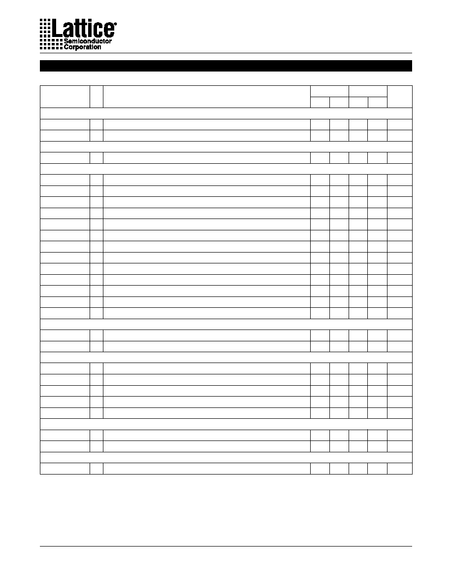
Specifications ispLSI 2192VE
7
USE
2192VE-225
FOR
NEW
DESIGNS
Internal Timing Parameters1
Over Recommended Operating Conditions
tio
1. Internal Timing Parameters are not tested and are for reference only.
2. Refer to Timing Model in this data sheet for further details.
3. The XOR adjacent path can only be used by hard macros.
Table 2-0036E/2192VE v0.1
Inputs
UNITS
-225
MIN. MAX.
DESCRIPTION
#
2
PARAMETER
20 Input Buffer Delay
ns
tdin
21 Dedicated Input Delay
ns
tgrp
22 GRP Delay
ns
GLB
t1ptxor
25 1 Product Term/XOR Path Delay
ns
t20ptxor
26 20 Product Term/XOR Path Delay
ns
txoradj
27 XOR Adjacent Path Delay
ns
tgbp
28 GLB Register Bypass Delay
ns
tgsu
29 GLB Register Setup Time before Clock
ns
tgh
30 GLB Register Hold Time after Clock
ns
tgco
31 GLB Register Clock to Output Delay
ns
3
tgro
32 GLB Register Reset to Output Delay
ns
tptre
33 GLB Product Term Reset to Register Delay
ns
tptoe
34 GLB Product Term Output Enable to I/O Cell Delay
ns
tptck
35 GLB Product Term Clock Delay
ns
ORP
tob
38 Output Buffer Delay
ns
tsl
39 Output Slew Limited Delay Adder
ns
GRP
t4ptbpc
23 4 Product Term Bypass Path Delay (Combinatorial)
ns
t4ptbpr
24 4 Product Term Bypass Path Delay (Registered)
ns
torp
36 ORP Delay
ns
torpbp
37 ORP Bypass Delay
ns
Outputs
toen
40 I/O Cell OE to Output Enabled
ns
todis
41 I/O Cell OE to Output Disabled
ns
tgoe
42 Global Output Enable
ns
tgy0
43 Clock Delay, Y0 to Global GLB Clock Line (Ref. clock)
ns
tgy1/2
44 Clock Delay, Y1 or Y2 to Global GLB Clock Line
ns
Clocks
tgr
45 Global Reset to GLB
0.3
0.5
0.2
3.2
0.0
–
0.3
4.0
2.9
3.2
1.6
2.0
1.5
2.2
0.9
0.4
2.6
1.9
0.9
1.1
3.7
–
0.7
1.8
–
0.8
–
0.9
1.1
–ns
Global Reset
-180
MIN. MAX.
0.5
1.1
0.6
3.4
0.0
–
0.3
0.6
4.3
5.9
4.0
1.6
2.0
1.9
2.4
1.4
0.4
3.0
2.0
1.2
1.4
4.4
–
1.2
2.3
–
1.0
–
1.2
1.4
–
相關(guān)PDF資料 |
PDF描述 |
|---|---|
| P51-50-A-J-D-4.5V-000-000 | SENSOR 50PSI 3/8-24UNF .5-4.5V |
| REC3-483.3DRWZ/H2/A/M | CONV DC/DC 3W 18-72VIN +/-3.3V |
| P51-1500-A-F-D-4.5OVP-000-000 | SENSOR 1500PSI 1/4-18NPT .5-4.5V |
| P51-300-A-Z-I12-20MA-000-000 | SENSOR 300PSI 1/4-18NPT 4-20MA |
| REC3-4815DRWZ/H2/C/M | CONV DC/DC 3W 18-72VIN +/-15VOUT |
相關(guān)代理商/技術(shù)參數(shù) |
參數(shù)描述 |
|---|---|
| ISPLSI2192VE-100LTN128 | 功能描述:CPLD - 復(fù)雜可編程邏輯器件 RoHS:否 制造商:Lattice 系列: 存儲類型:EEPROM 大電池數(shù)量:128 最大工作頻率:333 MHz 延遲時間:2.7 ns 可編程輸入/輸出端數(shù)量:64 工作電源電壓:3.3 V 最大工作溫度:+ 90 C 最小工作溫度:0 C 封裝 / 箱體:TQFP-100 |
| ISPLSI2192VE100LTN128I | 制造商:LATTICE 制造商全稱:Lattice Semiconductor 功能描述:3.3V In-System Programmable SuperFAST⑩ High Density PLD |
| ISPLSI2192VE135LB144 | 制造商:LATTICE 制造商全稱:Lattice Semiconductor 功能描述:3.3V In-System Programmable SuperFAST⑩ High Density PLD |
| ISPLSI2192VE-135LB144 | 功能描述:CPLD - 復(fù)雜可編程邏輯器件 RoHS:否 制造商:Lattice 系列: 存儲類型:EEPROM 大電池數(shù)量:128 最大工作頻率:333 MHz 延遲時間:2.7 ns 可編程輸入/輸出端數(shù)量:64 工作電源電壓:3.3 V 最大工作溫度:+ 90 C 最小工作溫度:0 C 封裝 / 箱體:TQFP-100 |
| ISPLSI2192VE-135-LB144 | 制造商:LATTICE 制造商全稱:Lattice Semiconductor 功能描述:3.3V In-System Programmable SuperFAST⑩ High Density PLD |
發(fā)布緊急采購,3分鐘左右您將得到回復(fù)。