- 您現(xiàn)在的位置:買賣IC網(wǎng) > PDF目錄21026 > ISPLSI 2192VE-100LTN128 (Lattice Semiconductor Corporation)IC PLD ISP 96I/O 10NS 128TQFP PDF資料下載
參數(shù)資料
| 型號(hào): | ISPLSI 2192VE-100LTN128 |
| 廠商: | Lattice Semiconductor Corporation |
| 文件頁數(shù): | 8/15頁 |
| 文件大小: | 0K |
| 描述: | IC PLD ISP 96I/O 10NS 128TQFP |
| 標(biāo)準(zhǔn)包裝: | 90 |
| 系列: | ispLSI® 2000VE |
| 可編程類型: | 系統(tǒng)內(nèi)可編程 |
| 最大延遲時(shí)間 tpd(1): | 10.0ns |
| 電壓電源 - 內(nèi)部: | 3 V ~ 3.6 V |
| 邏輯元件/邏輯塊數(shù)目: | 48 |
| 宏單元數(shù): | 192 |
| 門數(shù): | 8000 |
| 輸入/輸出數(shù): | 96 |
| 工作溫度: | 0°C ~ 70°C |
| 安裝類型: | 表面貼裝 |
| 封裝/外殼: | 128-LQFP |
| 供應(yīng)商設(shè)備封裝: | 128-TQFP(14x14) |
| 包裝: | 托盤 |
| 其它名稱: | 220-1623 ISPLSI 2192VE-100LTN128-ND ISPLSI2192VE-100LTN128 |
Specifications ispLSI 2192VE
2
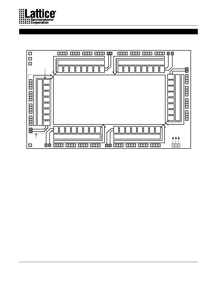
Functional Block Diagram
Figure 1. ispLSI 2192VE Functional Block Diagram
The 2192VE contains 96 I/O cells. Each I/O cell is directly
connected to an I/O pin and can be individually pro-
grammed to be a combinatorial input, output or
bi-directional I/O pin with 3-state control. The signal
levels are TTL compatible voltages and the output drivers
can source 4mA or sink 8mA. Each output can be
programmed independently for fast or slow output slew
rate to minimize overall output switching noise. Device
pins can be safely driven to 5V signal levels to support
mixed-voltage systems.
Eight GLBs, 16 I/O cells, two dedicated inputs and an
ORP are connected together to make a Megablock (see
Figure 1). The outputs of the eight GLBs are connected
to a set of 16 universal I/O cells by the ORP. Each ispLSI
2192VE device contains six Megablocks.
The GRP has as its inputs, the outputs from all of the
GLBs and all of the inputs from the bi-directional I/O cells.
All of these signals are made available to the inputs of the
GLBs. Delays through the GRP have been equalized to
minimize timing skew.
Clocks in the ispLSI 2192VE device are selected using
the dedicated clock pins. Three dedicated clock pins (Y0,
Y1, Y2) or an asynchronous clock can be selected on a
GLB basis. The asynchronous or Product Term clock
can be generated in any GLB for its own clock.
Programmable Open-Drain Outputs
In addition to the standard output configuration, the
outputs of the ispLSI 2192VE are individually program-
mable, either as a standard totem-pole output or an
open-drain output. The totem-pole output drives the
specified Voh and Vol levels, whereas the open-drain
output drives only the specified Vol. The Voh level on the
open-drain output depends on the external loading and
pull-up. This output configuration is controlled by a pro-
grammable fuse. The default configuration when the
device is in bulk erased state is totem-pole configuration.
The open-drain/totem-pole option is selectable through
the Lattice software tools.
Output Routing Pool (ORP)
B0
B1
B2
B3
B4
B5
B6
B7
Output Routing Pool (ORP)
C0
C1
C2
C3
C4
C5
C6
C7
Output Routing Pool (ORP)
F7
F6
F5
F4
F3
F2
F1
F0
Input Bus
Output Routing Pool (ORP)
E7
E6
E5
E4
E3
E2
E1
E0
Input Bus
A0
A1
A2
A3
A4
A5
A6
A7
Output
Routing
Pool
(ORP)
Generic
Logic Blocks
(GLBs)
Megablock
Input
Bus
Global
Routing
Pool
(GRP)
D7
D6
D5
D4
D3
D2
D1
D0
Output
Routing
Pool
(ORP)
I/O
94
I/O
95
I/O
93
I/O
92
I/O
91
I/O
90
I/O
89
I/O
88
I/O
87
I/O
86
I/O
85
I/O
84
I/O
83
I/O
82
I/O
81
I/O
80
IN
11*
I/O
78
I/O
79
I/O
77
I/O
76
I/O
75
I/O
74
I/O
73
I/O
72
I/O
71
I/O
70
I/O
69
I/O
68
I/O
67
I/O
66
I/O
65
I/O
64
IN
9
IN
10
I/O
17
I/O
16
I/O
18
I/O
19
I/O
20
I/O
21
I/O
22
I/O
23
I/O
24
I/O
25
I/O
26
I/O
27
I/O
28
I/O
29
I/O
30
I/O
31
IN 3
I/O
33
I/O
32
I/O
34
I/O
35
I/O
36
I/O
37
I/O
38
I/O
39
I/O
40
I/O
41
I/O
42
I/O
43
I/O
44
I/O
45
I/O
46
Y0 Y1 Y2
I/O
47
IN 5*
IN4
IN 7/TCK
IN 6/TDO
I/O 63
I/O 62
I/O 61
I/O 60
I/O 59
I/O 58
I/O 57
I/O 56
I/O 55
I/O 54
I/O 53
I/O 52
I/O 51
I/O 50
I/O 49
I/O 48
I/O 0
I/O 1
I/O 2
I/O 3
I/O 6
I/O 7
I/O 8
I/O 9
I/O 10
I/O 11
I/O 12
I/O 13
I/O 14
I/O 15
TDI/IN 0
TMS/IN 1
I/O 4
I/O 5
BSCAN
RESET
Input Bus
lnput
Bus
2192VE Block.eps
IN
8
GOE 0
GOE 1
IN 2*
*Note: Dedicated Inputs 2, 5 and 11 are not available with 128-pin packages.
CLK
0
CLK
1
CLK
2
相關(guān)PDF資料 |
PDF描述 |
|---|---|
| P51-50-A-J-D-4.5V-000-000 | SENSOR 50PSI 3/8-24UNF .5-4.5V |
| REC3-483.3DRWZ/H2/A/M | CONV DC/DC 3W 18-72VIN +/-3.3V |
| P51-1500-A-F-D-4.5OVP-000-000 | SENSOR 1500PSI 1/4-18NPT .5-4.5V |
| P51-300-A-Z-I12-20MA-000-000 | SENSOR 300PSI 1/4-18NPT 4-20MA |
| REC3-4815DRWZ/H2/C/M | CONV DC/DC 3W 18-72VIN +/-15VOUT |
相關(guān)代理商/技術(shù)參數(shù) |
參數(shù)描述 |
|---|---|
| ISPLSI2192VE-100LTN128 | 功能描述:CPLD - 復(fù)雜可編程邏輯器件 RoHS:否 制造商:Lattice 系列: 存儲(chǔ)類型:EEPROM 大電池?cái)?shù)量:128 最大工作頻率:333 MHz 延遲時(shí)間:2.7 ns 可編程輸入/輸出端數(shù)量:64 工作電源電壓:3.3 V 最大工作溫度:+ 90 C 最小工作溫度:0 C 封裝 / 箱體:TQFP-100 |
| ISPLSI2192VE100LTN128I | 制造商:LATTICE 制造商全稱:Lattice Semiconductor 功能描述:3.3V In-System Programmable SuperFAST⑩ High Density PLD |
| ISPLSI2192VE135LB144 | 制造商:LATTICE 制造商全稱:Lattice Semiconductor 功能描述:3.3V In-System Programmable SuperFAST⑩ High Density PLD |
| ISPLSI2192VE-135LB144 | 功能描述:CPLD - 復(fù)雜可編程邏輯器件 RoHS:否 制造商:Lattice 系列: 存儲(chǔ)類型:EEPROM 大電池?cái)?shù)量:128 最大工作頻率:333 MHz 延遲時(shí)間:2.7 ns 可編程輸入/輸出端數(shù)量:64 工作電源電壓:3.3 V 最大工作溫度:+ 90 C 最小工作溫度:0 C 封裝 / 箱體:TQFP-100 |
| ISPLSI2192VE-135-LB144 | 制造商:LATTICE 制造商全稱:Lattice Semiconductor 功能描述:3.3V In-System Programmable SuperFAST⑩ High Density PLD |
發(fā)布緊急采購,3分鐘左右您將得到回復(fù)。