- 您現在的位置:買賣IC網 > Datasheet目錄42 > LTC4260IUH#PBF (Linear Technology)IC HOT SWAP CNTRL I2C 32-QFN Datasheet資料下載
參數資料
| 型號: | LTC4260IUH#PBF |
| 廠商: | Linear Technology |
| 文件頁數: | 11/30頁 |
| 文件大小: | 295K |
| 描述: | IC HOT SWAP CNTRL I2C 32-QFN |
| 標準包裝: | 73 |
| 類型: | 熱交換控制器 |
| 應用: | 通用 |
| 內部開關: | 無 |
| 電源電壓: | 8.5 V ~ 80 V |
| 工作溫度: | -40°C ~ 85°C |
| 安裝類型: | 表面貼裝 |
| 封裝/外殼: | 32-WFQFN 裸露焊盤 |
| 供應商設備封裝: | 32-QFN 裸露焊盤(5x5) |
| 包裝: | 管件 |
第1頁第2頁第3頁第4頁第5頁第6頁第7頁第8頁第9頁第10頁當前第11頁第12頁第13頁第14頁第15頁第16頁第17頁第18頁第19頁第20頁第21頁第22頁第23頁第24頁第25頁第26頁第27頁第28頁第29頁第30頁
LTC4260
11
4260fc
For more information www.linear.com/LTC4260
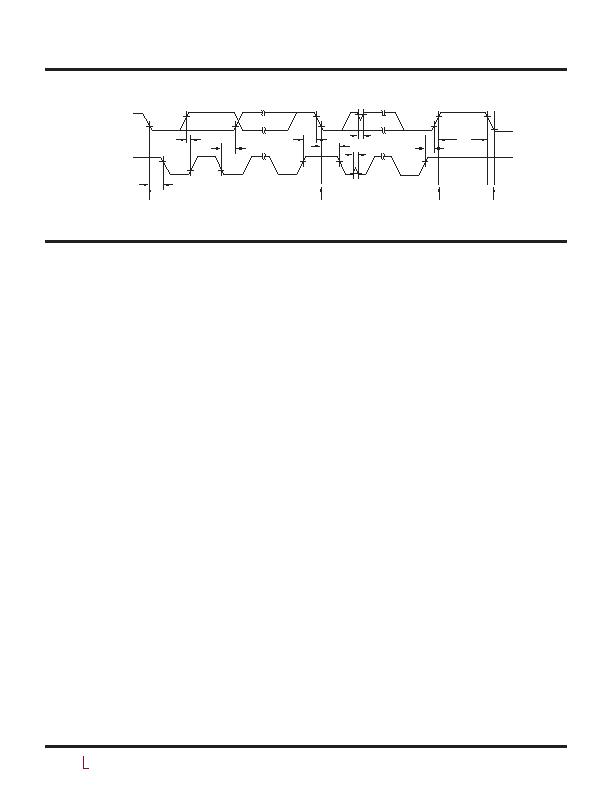
TiMing DiagraM
operaTion
The Functional Diagram displays the main functional areas
of this device. The LTC4260 is designed to turn a boards
supply voltage on and off in a controlled manner, allowing
the board to be safely inserted or removed from a live
backplane. During normal operation, the charge pump
and gate driver turn on the external N-channel pass FETs
gate to pass power to the load. The gate driver uses a
charge pump that derives its power from the SOURCE pin.
When the SOURCE pin is at ground, the charge pump is
powered from an internal 12V supply derived from V
DD
.
This results in a 200礎 current load on the SOURCE pin
when the gate is up. Also included in the gate driver is an
internal 15V gate-to-source clamp.
The current sense (CS) amplifier monitors the load cur-
rent using the difference between the V
DD
and SENSE pin
voltage. The CS amplifier limits the current in the load by
reducing the GATE-to-SOURCE voltage in an active control
loop. The CS amplifier requires 100礎 input bias current
from both the V
DD
and the SENSE pins.
A short circuit on the output to ground causes significant
power dissipation during active current limiting. To limit
this power, the foldback amplifier reduces the current limit
value from 50mV to 20mV (referred to the V
DD
minus
SENSE voltage) in a linear manner as the FB pin drops
below 2V (see Typical Performance curves).
If an overcurrent condition persists, the TIMER pin ramps
up with a 100礎 current source until the pin voltage
exceeds 1.2V (comparator TM2). This indicates to the
logic that it is time to turn off the pass FET to prevent
overheating. At this point the TIMER pin ramps down us-
ing the 2礎 current source until the voltage drops below
t
SU, DAT
t
SU, STO
t
SU, STA
t
BUF
t
HD, STA
t
SP
t
SP
t
HD, DATO,
t
HD, DATI
t
HD, STA
START
NDITI N
STOP
NDITI N
REPEATED START
NDITI N
START
NDITI N
4260 TD01
SDAI/SDAO
SCL
0.2V (comparator TM1) which tells the logic that the pass
transistor has cooled and it is safe to turn it on again.
The output voltage is monitored using the FB pin and the
PG comparator to determine if the power is available for
the load. The power good condition is signalled by the
GPIO pin using an open-drain pull-down transistor. The
GPIO pin can also be used as a general purpose input (GP
comparator) or output pin.
The Functional Diagram shows the monitoring blocks of
the LTC4260. The group of comparators on the left side
includes the UV, OV, RST, BP and ON comparators. These
comparators are used to determine if the external condi-
tions are valid prior to turning on the FET. But first the
two undervoltage lockout circuits UVLO1 and UVLO2 must
validate the input supply and the internally generated 5.5V
supply (INTV
CC
) and generate the power up initialization
to the logic circuits.
Included in the LTC4260 is an 8-bit A/D converter. The
converter has a 3-input mux to select between the ADIN
pin, the SOURCE pin and the V
DD
SENSE voltage.
An I
2
C interface is provided to read the A/D registers. It also
allows the host to poll the device and determine if faults
have occurred. If the ALERT line is used as an interrupt,
the host can respond to a fault in real time. The typical SDA
line is divided into an SDAI (input) and SDAO (output).
This simplifies applications using an optoisolator driven
directly from the SDAO output. The I
2
C device address is
decoded using the ADR0, ADR1 and ADR2 pins. These
inputs have three states each that decode into a total of
27 device addresses.
相關PDF資料 |
PDF描述 |
|---|---|
| LTC4261IGN-2#PBF | IC CTRLR HOTSWAP W/ADC 28-SSOP |
| LTC4263IS#TRPBF | IC IEEE 803.2AF CNTRLR 14-SOIC |
| LTC4268IDKD-1#PBF | IC PD HIGH POWER W/CNTRL 32-DFN |
| LTC4274CUHF#PBF | IC CONTROLLER POE 38-QFN |
| LTC4280CUFD#PBF | IC CONTROLLER HOT SWAP QFN-24 |
相關代理商/技術參數 |
參數描述 |
|---|---|
| LTC4261 | 制造商:LINER 制造商全稱:Linear Technology 功能描述:Negative Voltage Hot Swap Controllers with ADC and I2C Monitoring |
| LTC4261CGN | 功能描述:IC CTRLR HOTSWAP W/ADC 28-SSOP RoHS:否 類別:集成電路 (IC) >> PMIC - 熱交換 系列:- 產品培訓模塊:Lead (SnPb) Finish for COTS Obsolescence Mitigation Program 標準包裝:119 系列:- 類型:熱交換控制器 應用:通用型,PCI Express? 內部開關:無 電流限制:- 電源電壓:3.3V,12V 工作溫度:-40°C ~ 85°C 安裝類型:表面貼裝 封裝/外殼:80-TQFP 供應商設備封裝:80-TQFP(12x12) 包裝:托盤 產品目錄頁面:1423 (CN2011-ZH PDF) |
| LTC4261CGN#PBF | 功能描述:IC CTRLR HOTSWAP W/ADC 28-SSOP RoHS:是 類別:集成電路 (IC) >> PMIC - 熱交換 系列:- 產品培訓模塊:Lead (SnPb) Finish for COTS Obsolescence Mitigation Program 標準包裝:119 系列:- 類型:熱交換控制器 應用:通用型,PCI Express? 內部開關:無 電流限制:- 電源電壓:3.3V,12V 工作溫度:-40°C ~ 85°C 安裝類型:表面貼裝 封裝/外殼:80-TQFP 供應商設備封裝:80-TQFP(12x12) 包裝:托盤 產品目錄頁面:1423 (CN2011-ZH PDF) |
| LTC4261CGN#TR | 功能描述:IC CTRLR HOTSWAP W/ADC 28-SSOP RoHS:否 類別:集成電路 (IC) >> PMIC - 熱交換 系列:- 產品培訓模塊:Lead (SnPb) Finish for COTS Obsolescence Mitigation Program 標準包裝:119 系列:- 類型:熱交換控制器 應用:通用型,PCI Express? 內部開關:無 電流限制:- 電源電壓:3.3V,12V 工作溫度:-40°C ~ 85°C 安裝類型:表面貼裝 封裝/外殼:80-TQFP 供應商設備封裝:80-TQFP(12x12) 包裝:托盤 產品目錄頁面:1423 (CN2011-ZH PDF) |
| LTC4261CGN#TRPBF | 功能描述:IC CTRLR HOTSWAP W/ADC 28-SSOP RoHS:是 類別:集成電路 (IC) >> PMIC - 熱交換 系列:- 產品培訓模塊:Lead (SnPb) Finish for COTS Obsolescence Mitigation Program 標準包裝:119 系列:- 類型:熱交換控制器 應用:通用型,PCI Express? 內部開關:無 電流限制:- 電源電壓:3.3V,12V 工作溫度:-40°C ~ 85°C 安裝類型:表面貼裝 封裝/外殼:80-TQFP 供應商設備封裝:80-TQFP(12x12) 包裝:托盤 產品目錄頁面:1423 (CN2011-ZH PDF) |
發布緊急采購,3分鐘左右您將得到回復。