- 您現(xiàn)在的位置:買賣IC網(wǎng) > PDF目錄371047 > MC68HC08AS32 (Motorola, Inc.) 8-Bit Microcontroller Units (MCUs) With Embedded EEPROM For User Data Storage(8位微控制器單元(MCUs),帶嵌入式EEPROM數(shù)據(jù)存儲單元) PDF資料下載
參數(shù)資料
| 型號: | MC68HC08AS32 |
| 廠商: | Motorola, Inc. |
| 英文描述: | 8-Bit Microcontroller Units (MCUs) With Embedded EEPROM For User Data Storage(8位微控制器單元(MCUs),帶嵌入式EEPROM數(shù)據(jù)存儲單元) |
| 中文描述: | 8位微控制器單元(MCU)與嵌入式對于用戶數(shù)據(jù)存儲(8位微控制器單元(MCU)的,帶嵌入式EEPROM的數(shù)據(jù)存儲單元的EEPROM) |
| 文件頁數(shù): | 374/394頁 |
| 文件大小: | 3174K |
| 代理商: | MC68HC08AS32 |
第1頁第2頁第3頁第4頁第5頁第6頁第7頁第8頁第9頁第10頁第11頁第12頁第13頁第14頁第15頁第16頁第17頁第18頁第19頁第20頁第21頁第22頁第23頁第24頁第25頁第26頁第27頁第28頁第29頁第30頁第31頁第32頁第33頁第34頁第35頁第36頁第37頁第38頁第39頁第40頁第41頁第42頁第43頁第44頁第45頁第46頁第47頁第48頁第49頁第50頁第51頁第52頁第53頁第54頁第55頁第56頁第57頁第58頁第59頁第60頁第61頁第62頁第63頁第64頁第65頁第66頁第67頁第68頁第69頁第70頁第71頁第72頁第73頁第74頁第75頁第76頁第77頁第78頁第79頁第80頁第81頁第82頁第83頁第84頁第85頁第86頁第87頁第88頁第89頁第90頁第91頁第92頁第93頁第94頁第95頁第96頁第97頁第98頁第99頁第100頁第101頁第102頁第103頁第104頁第105頁第106頁第107頁第108頁第109頁第110頁第111頁第112頁第113頁第114頁第115頁第116頁第117頁第118頁第119頁第120頁第121頁第122頁第123頁第124頁第125頁第126頁第127頁第128頁第129頁第130頁第131頁第132頁第133頁第134頁第135頁第136頁第137頁第138頁第139頁第140頁第141頁第142頁第143頁第144頁第145頁第146頁第147頁第148頁第149頁第150頁第151頁第152頁第153頁第154頁第155頁第156頁第157頁第158頁第159頁第160頁第161頁第162頁第163頁第164頁第165頁第166頁第167頁第168頁第169頁第170頁第171頁第172頁第173頁第174頁第175頁第176頁第177頁第178頁第179頁第180頁第181頁第182頁第183頁第184頁第185頁第186頁第187頁第188頁第189頁第190頁第191頁第192頁第193頁第194頁第195頁第196頁第197頁第198頁第199頁第200頁第201頁第202頁第203頁第204頁第205頁第206頁第207頁第208頁第209頁第210頁第211頁第212頁第213頁第214頁第215頁第216頁第217頁第218頁第219頁第220頁第221頁第222頁第223頁第224頁第225頁第226頁第227頁第228頁第229頁第230頁第231頁第232頁第233頁第234頁第235頁第236頁第237頁第238頁第239頁第240頁第241頁第242頁第243頁第244頁第245頁第246頁第247頁第248頁第249頁第250頁第251頁第252頁第253頁第254頁第255頁第256頁第257頁第258頁第259頁第260頁第261頁第262頁第263頁第264頁第265頁第266頁第267頁第268頁第269頁第270頁第271頁第272頁第273頁第274頁第275頁第276頁第277頁第278頁第279頁第280頁第281頁第282頁第283頁第284頁第285頁第286頁第287頁第288頁第289頁第290頁第291頁第292頁第293頁第294頁第295頁第296頁第297頁第298頁第299頁第300頁第301頁第302頁第303頁第304頁第305頁第306頁第307頁第308頁第309頁第310頁第311頁第312頁第313頁第314頁第315頁第316頁第317頁第318頁第319頁第320頁第321頁第322頁第323頁第324頁第325頁第326頁第327頁第328頁第329頁第330頁第331頁第332頁第333頁第334頁第335頁第336頁第337頁第338頁第339頁第340頁第341頁第342頁第343頁第344頁第345頁第346頁第347頁第348頁第349頁第350頁第351頁第352頁第353頁第354頁第355頁第356頁第357頁第358頁第359頁第360頁第361頁第362頁第363頁第364頁第365頁第366頁第367頁第368頁第369頁第370頁第371頁第372頁第373頁當(dāng)前第374頁第375頁第376頁第377頁第378頁第379頁第380頁第381頁第382頁第383頁第384頁第385頁第386頁第387頁第388頁第389頁第390頁第391頁第392頁第393頁第394頁
L
G
R
Electrical Specifications
Advance Information
MC68HC08AS32
—
Rev. 3.0
374
Electrical Specifications
MOTOROLA
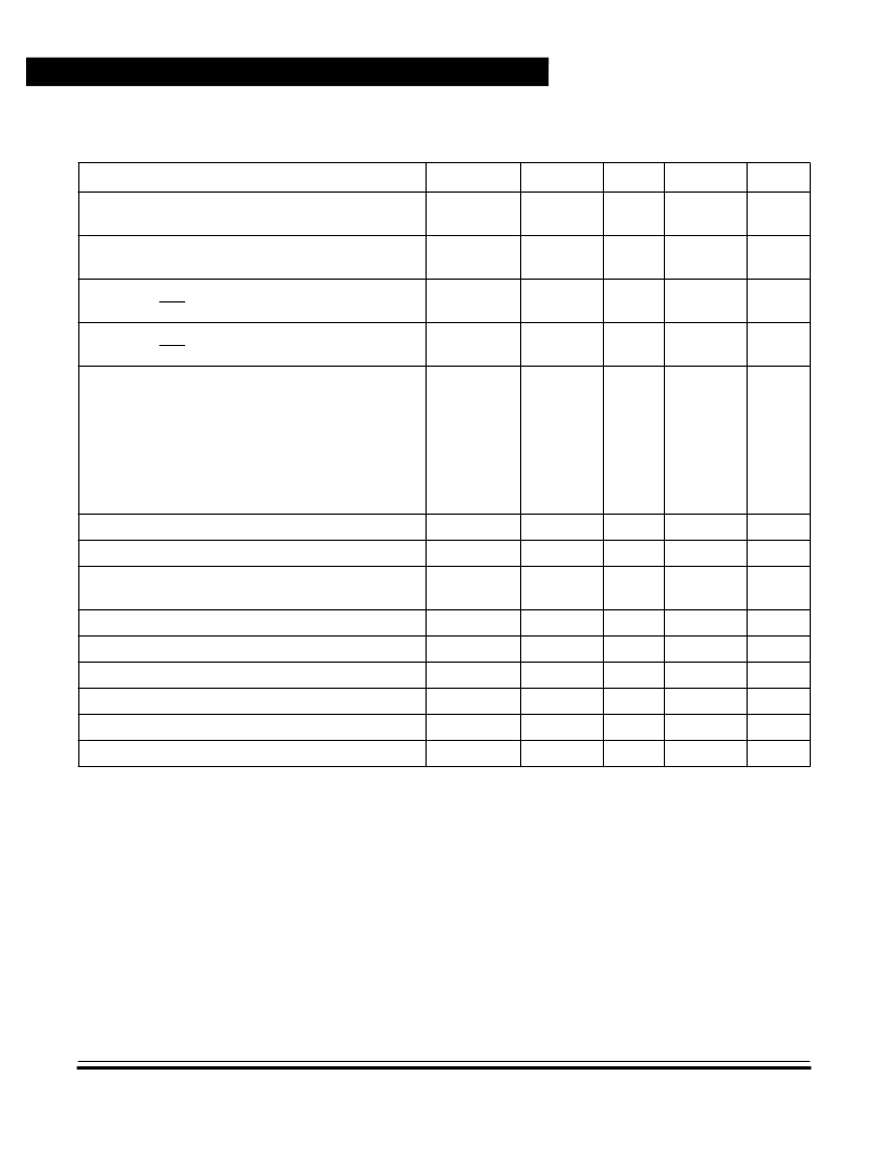
21.5 5.0-Volt DC Electrical Characteristics Control Timing
Characteristic
(1)
1. V
DD
= 5.0 Vdc
±
10%, V
SS
= 0 Vdc, T
A
= –40
°
C to +105
°
C, unless otherwise noted.
2. Typical values reflect average measurements at midpoint of voltage range, 25
°
C only.
3. Run (Operating) I
DD
measured using external square wave clock source (f
OP
= 8.4 MHz). All inputs 0.2 V from rail. No dc
loads. Less than 100 pF on all outputs. C
L
= 20 pF on OSC2. All ports configured as inputs. OSC2 capacitance linearly
affects run I
DD
. Measured with all modules enabled.
4. Wait I
DD
measuredusing external square wave clock source (f
OP
= 8.4 MHz). All inputs 0.2 Vdc from rail. No dcloads. Less
than 100 pF on all outputs, C
L
= 20 pF on OSC2. All ports configured as inputs. OSC2 capacitance linearly affects wait
I
DD
. Measured with all modules enabled.
5. Stop I
DD
measured with OSC1 = V
SS
.
6. Maximum is highest voltage that POR is guaranteed.
7. Maximum is highest voltage that POR is possible.
8. If minimum V
DD
is not reached before the internal POR reset is released, RST must be driven low externally until minimum
V
DD
is reached.
9. See
13.9 COP Module During Break Interrupts
.
Symbol
Min
Typ
(2)
Max
Unit
Output High Voltage
(I
Load
= –2.0 mA) All Ports, RESET
Output Low Voltage
(I
Load
= 1.6 mA) All Ports, RESET
Input High Voltage
All Ports, IRQs, RESET, OSC1
V
OH
V
DD
–0.8
—
—
V
V
OL
—
—
0.4
V
V
IH
0.7 x V
DD
—
V
DD
V
Input Low Voltage
All Ports, IRQs, RESET, OSC1
V
IL
V
SS
—
0.3 x V
DD
V
V
DD
+ V
DDA
/V
DDAREF
Supply Current
Run
(3)
Wait
(4)
Stop
(5)
25
°
C
–40
°
C to +105
°
C
25
°
C with LVI Enabled
–40
°
C to +105
°
C with LVI Enabled
I
DD
—
—
—
—
—
—
—
—
—
—
—
—
30
15
5
50
400
500
mA
mA
μ
A
μ
A
μ
A
μ
A
μ
A
μ
A
I/O Ports Hi-Z Leakage Current
I
L
I
IN
—
—
±
1
±
1
Input Current
—
—
Capacitance
Ports (As Input or Output)
C
OUT
C
IN
V
LVF
H
LVI
V
POR
V
PORRST
R
POR
V
HI
—
—
—
—
12
8
pF
Low-Voltage Reset Inhibit
3.7
4.1
4.45
V
Low-Voltage Reset Inhibit/Recover Hysteresis
POR ReArm Voltage
(6)
POR Reset Voltage
(7)
POR Rise Time Ramp Rate
(8)
High COP Disable Voltage
(9)
50
150
—
mV
0
—
200
mV
0
—
800
mV
0.02
—
—
V/ms
V
DD
V
DD
+ 2
V
相關(guān)PDF資料 |
PDF描述 |
|---|---|
| MC68HC08AZ16 | HCMOS Microcontroller Unit |
| MC68HC08AZ24 | HCMOS Microcontroller Unit |
| MC68HC08AZ32 | 8-Bit Microcontroller Units (MCU).(8位微控制器) |
| MC68HC08AZ60AMFU | Microcontrollers |
| MC68HC08AZ60AVFU | CONTACT |
相關(guān)代理商/技術(shù)參數(shù) |
參數(shù)描述 |
|---|---|
| MC68HC08AZ0 | 制造商:MOTOROLA 制造商全稱:Motorola, Inc 功能描述:Advance Information |
| MC68HC08AZ0CFU | 制造商:MOTOROLA 制造商全稱:Motorola, Inc 功能描述:Advance Information |
| MC68HC08AZ16 | 制造商:MOTOROLA 制造商全稱:Motorola, Inc 功能描述:HCMOS Microcontroller Unit |
| MC68HC08AZ24 | 制造商:MOTOROLA 制造商全稱:Motorola, Inc 功能描述:HCMOS Microcontroller Unit |
| MC68HC08AZ32 | 制造商:FREESCALE 制造商全稱:Freescale Semiconductor, Inc 功能描述:Advance Information |
發(fā)布緊急采購,3分鐘左右您將得到回復(fù)。