- 您現在的位置:買賣IC網 > PDF目錄371126 > MMDF3N03HDR2 (ON SEMICONDUCTOR) Power MOSFET 3 Amps, 30 Volts PDF資料下載
參數資料
| 型號: | MMDF3N03HDR2 |
| 廠商: | ON SEMICONDUCTOR |
| 元件分類: | 功率晶體管 |
| 英文描述: | Power MOSFET 3 Amps, 30 Volts |
| 中文描述: | 4.1 A, 30 V, 0.07 ohm, N-CHANNEL, Si, POWER, MOSFET |
| 封裝: | MINIATURE, CASE 751-07, SOP-8 |
| 文件頁數: | 7/10頁 |
| 文件大小: | 281K |
| 代理商: | MMDF3N03HDR2 |
7
Motorola TMOS Power MOSFET Transistor Device Data
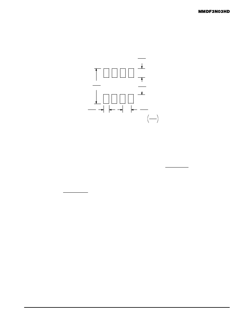
INFORMATION FOR USING THE SO–8 SURFACE MOUNT PACKAGE
MINIMUM RECOMMENDED FOOTPRINT FOR SURFACE MOUNTED APPLICATIONS
Surface mount board layout is a critical portion of the total
design. The footprint for the semiconductor packages must be
the correct size to ensure proper solder connection interface
between the board and the package. With the correct pad
geometry, the packages will self–align when subjected to a
solder reflow process.
mm
inches
0.060
1.52
0.275
7.0
0.024
0.6
0.050
1.270
0.155
4.0
SO–8 POWER DISSIPATION
The power dissipation of the SO–8 is a function of the input
pad size. This can vary from the minimum pad size for
soldering to the pad size given for maximum power
dissipation. Power dissipation for a surface mount device is
determined by TJ(max), the maximum rated junction
temperature of the die, R
θ
JA, the thermal resistance from the
device junction to ambient; and the operating temperature, TA.
Using the values provided on the data sheet for the SO–8
package, PD can be calculated as follows:
PD =
TJ(max) – TA
R
θ
JA
The values for the equation are found in the maximum
ratings table on the data sheet. Substituting these values into
the equation for an ambient temperature TA of 25
°
C, one can
calculate the power dissipation of the device which in this case
is 2.0 Watts.
PD =
150
°
C – 25
°
C
62.5
°
C/W
= 2.0 Watts
The 62.5
°
C/W for the SO–8 package assumes the
recommended footprint on a glass epoxy printed circuit board
to achieve a power dissipation of 2.0 Watts using the footprint
shown. Another alternative would be to use a ceramic
substrate or an aluminum core board such as Thermal Clad
.
Using board material such as Thermal Clad, the power
dissipation can be doubled using the same footprint.
SOLDERING PRECAUTIONS
The melting temperature of solder is higher than the rated
temperature of the device. When the entire device is heated
to a high temperature, failure to complete soldering within a
short time could result in device failure. Therefore, the
following items should always be observed in order to
minimize the thermal stress to which the devices are
subjected.
Always preheat the device.
The delta temperature between the preheat and soldering
should be 100
°
C or less.*
When preheating and soldering, the temperature of the
leads and the case must not exceed the maximum
temperature ratings as shown on the data sheet. When
using infrared heating with the reflow soldering method,
the difference shall be a maximum of 10
°
C.
The soldering temperature and time shall not exceed
260
°
C for more than 10 seconds.
When shifting from preheating to soldering, the maximum
temperature gradient shall be 5
°
C or less.
After soldering has been completed, the device should be
allowed to cool naturally for at least three minutes.
Gradual cooling should be used as the use of forced
cooling will increase the temperature gradient and result
in latent failure due to mechanical stress.
Mechanical stress or shock should not be applied during
cooling.
* Soldering a device without preheating can cause excessive
thermal shock and stress which can result in damage to the
device.
相關PDF資料 |
PDF描述 |
|---|---|
| MMDF4N01HD | DUAL TMOS POWER MOSFET 4.0 AMPERES 20 VOLTS |
| MMDF6N02HD | DUAL TMOS POWER MOSFET 6.0 AMPERES 20 VOLTS |
| MMFR-29C516E-31SB | 16 Bit Flow Through EDAC Error Detection And Correction unit |
| MMKR-29C516E-31SB | 16 Bit Flow Through EDAC Error Detection And Correction unit |
| MMFT1N10E | MEDIUM POWER TMOS FET 1 AMP 100 VOLTS |
相關代理商/技術參數 |
參數描述 |
|---|---|
| MMDF3N04HD | 制造商:ONSEMI 制造商全稱:ON Semiconductor 功能描述:Power MOSFET 3 Amps, 40 Volts |
| MMDF3N04HDR2 | 功能描述:MOSFET 40V 3A N-Channel RoHS:否 制造商:STMicroelectronics 晶體管極性:N-Channel 汲極/源極擊穿電壓:650 V 閘/源擊穿電壓:25 V 漏極連續電流:130 A 電阻汲極/源極 RDS(導通):0.014 Ohms 配置:Single 最大工作溫度: 安裝風格:Through Hole 封裝 / 箱體:Max247 封裝:Tube |
| MMDF3N04HDR2G | 功能描述:MOSFET NFET SO8D 40V 3.4A 80mOhm RoHS:否 制造商:STMicroelectronics 晶體管極性:N-Channel 汲極/源極擊穿電壓:650 V 閘/源擊穿電壓:25 V 漏極連續電流:130 A 電阻汲極/源極 RDS(導通):0.014 Ohms 配置:Single 最大工作溫度: 安裝風格:Through Hole 封裝 / 箱體:Max247 封裝:Tube |
| MMDF3N06HD | 制造商:MOTOROLA 制造商全稱:Motorola, Inc 功能描述:DUAL TMOS POWER MOSFET 60 VOLTS |
| MMDF3N06VL | 制造商:ONSEMI 制造商全稱:ON Semiconductor 功能描述:Power MOSFET 3 Amps, 60 Volts N−Channel SO−8, Dual |
發布緊急采購,3分鐘左右您將得到回復。