- 您現(xiàn)在的位置:買賣IC網(wǎng) > PDF目錄371126 > MMFT5P03HD (ON SEMICONDUCTOR) 30V N-Channel PowerTrench MOSFET PDF資料下載
參數(shù)資料
| 型號(hào): | MMFT5P03HD |
| 廠商: | ON SEMICONDUCTOR |
| 元件分類: | 功率晶體管 |
| 英文描述: | 30V N-Channel PowerTrench MOSFET |
| 中文描述: | 3.7 A, 30 V, 0.1 ohm, P-CHANNEL, Si, POWER, MOSFET, TO-261AA |
| 封裝: | CASE 318E-04, 4 PIN |
| 文件頁(yè)數(shù): | 7/12頁(yè) |
| 文件大小: | 198K |
| 代理商: | MMFT5P03HD |
7
Motorola TMOS Power MOSFET Transistor Device Data
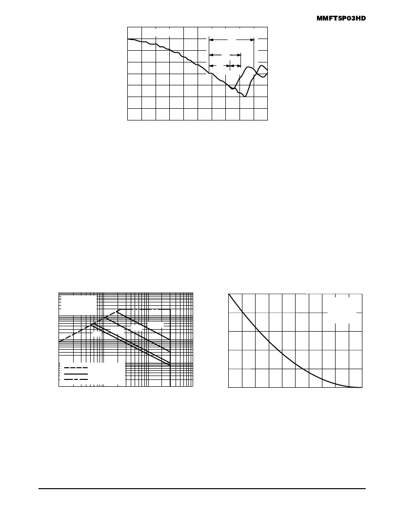
I
t, TIME
Figure 11. Reverse Recovery Time (trr)
di/dt = 300 A/
μ
s
Standard Cell Density
trr
High Cell Density
trr
tb
ta
SAFE OPERATING AREA
The Forward Biased Safe Operating Area curves define
the maximum simultaneous drain–to–source voltage and
drain current that a transistor can handle safely when it is for-
ward biased. Curves are based upon maximum peak junc-
tion temperature and a case temperature (TC) of 25
°
C. Peak
repetitive pulsed power limits are determined by using the
thermal response data in conjunction with the procedures
discussed in AN569, “Transient Thermal Resistance – Gen-
eral Data and Its Use.”
Switching between the off–state and the on–state may tra-
verse any load line provided neither rated peak current (IDM)
nor rated voltage (VDSS) is exceeded, and that the transition
time (tr, tf) does not exceed 10
μ
s. In addition the total power
averaged over a complete switching cycle must not exceed
(TJ(MAX) – TC)/(R
θ
JC).
A power MOSFET designated E–FET can be safely used
in switching circuits with unclamped inductive loads. For reli-
able operation, the stored energy from circuit inductance dis-
sipated in the transistor while in avalanche must be less than
the rated limit and must be adjusted for operating conditions
differing from those specified. Although industry practice is to
rate in terms of energy, avalanche energy capability is not a
constant. The energy rating decreases non–linearly with an
increase of peak current in avalanche and peak junction tem-
perature.
Figure 12. Maximum Rated Forward Biased
Safe Operating Area
0.1
VDS, DRAIN–TO–SOURCE VOLTAGE (VOLTS)
1
10
I
RDS(on) LIMIT
THERMAL LIMIT
PACKAGE LIMIT
0.01
VGS = 20 V
SINGLE PULSE
TC = 25
°
C
10
0.1
dc
10 ms
1
100
100
1 ms
Figure 13. Maximum Avalanche Energy versus
Starting Junction Temperature
TJ, STARTING JUNCTION TEMPERATURE (
°
C)
EA
A
25
50
75
100
125
VDD = 30 V
VGS = 10 V
IL = 12 Apk
L = 3.5 mH
150
0
150
50
100
200
250
100
μ
s
相關(guān)PDF資料 |
PDF描述 |
|---|---|
| MMFT5P03HDT3 | 30V N-Channel PowerTrench MOSFET |
| MMFT5P03HD | TMOS MEDIUM POWER FET 5.2 AMPERES 30 VOLTS |
| MMG05N60D | POWERLUX IGBT |
| MMG05N60D | Insulated Gate Bipolar Transistor |
| MMPQ2222 | Quad General Purpose Transistors |
相關(guān)代理商/技術(shù)參數(shù) |
參數(shù)描述 |
|---|---|
| MMFT5P03HDT1 | 功能描述:MOSFET P-CH 30V 3.7A SOT223 RoHS:否 類別:分離式半導(dǎo)體產(chǎn)品 >> FET - 單 系列:- 標(biāo)準(zhǔn)包裝:1,000 系列:MESH OVERLAY™ FET 型:MOSFET N 通道,金屬氧化物 FET 特點(diǎn):邏輯電平門 漏極至源極電壓(Vdss):200V 電流 - 連續(xù)漏極(Id) @ 25° C:18A 開態(tài)Rds(最大)@ Id, Vgs @ 25° C:180 毫歐 @ 9A,10V Id 時(shí)的 Vgs(th)(最大):4V @ 250µA 閘電荷(Qg) @ Vgs:72nC @ 10V 輸入電容 (Ciss) @ Vds:1560pF @ 25V 功率 - 最大:40W 安裝類型:通孔 封裝/外殼:TO-220-3 整包 供應(yīng)商設(shè)備封裝:TO-220FP 包裝:管件 |
| MMFT5P03HDT3 | 制造商:MOTOROLA 制造商全稱:Motorola, Inc 功能描述:TMOS P-CHANNEL FIELD FEECT TRANSISTOR |
| MMFT6N03HD | 制造商:MOTOROLA 制造商全稱:Motorola, Inc 功能描述:TMOS POWER 6.0 AMPERES 30 VOLTS |
| MMFT960T1 | 功能描述:MOSFET 60V 300mA N-Channel RoHS:否 制造商:STMicroelectronics 晶體管極性:N-Channel 汲極/源極擊穿電壓:650 V 閘/源擊穿電壓:25 V 漏極連續(xù)電流:130 A 電阻汲極/源極 RDS(導(dǎo)通):0.014 Ohms 配置:Single 最大工作溫度: 安裝風(fēng)格:Through Hole 封裝 / 箱體:Max247 封裝:Tube |
| MMFT960T1_06 | 制造商:ONSEMI 制造商全稱:ON Semiconductor 功能描述:Power MOSFET 300 mA, 60 Volts N−Channel SOT−223 |
發(fā)布緊急采購(gòu),3分鐘左右您將得到回復(fù)。