- 您現在的位置:買賣IC網 > PDF目錄371126 > MMSF5N03HD (MOTOROLA INC) SINGLE TMOS POWER MOSFET 5.0 AMPERES 30 VOLTS PDF資料下載
參數資料
| 型號: | MMSF5N03HD |
| 廠商: | MOTOROLA INC |
| 元件分類: | JFETs |
| 英文描述: | SINGLE TMOS POWER MOSFET 5.0 AMPERES 30 VOLTS |
| 中文描述: | 5 A, 30 V, 0.045 ohm, 2 CHANNEL, N-CHANNEL, Si, POWER, MOSFET |
| 封裝: | CASE 751-05, SOIC-8 |
| 文件頁數: | 6/10頁 |
| 文件大小: | 294K |
| 代理商: | MMSF5N03HD |
6
Motorola TMOS Power MOSFET Transistor Device Data
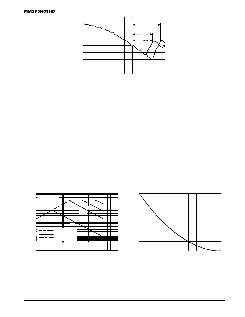
I
t, TIME
Figure 11. Reverse Recovery Time (trr)
di/dt = 300 A/
μ
s
Standard Cell Density
trr
High Cell Density
trr
tb
ta
SAFE OPERATING AREA
The Forward Biased Safe Operating Area curves define
the maximum simultaneous drain–to–source voltage and
drain current that a transistor can handle safely when it is for-
ward biased. Curves are based upon maximum peak junc-
tion temperature and a case temperature (TC) of 25
°
C. Peak
repetitive pulsed power limits are determined by using the
thermal response data in conjunction with the procedures
discussed in AN569, “Transient Thermal Resistance – Gen-
eral Data and Its Use.”
Switching between the off–state and the on–state may tra-
verse any load line provided neither rated peak current (IDM)
nor rated voltage (VDSS) is exceeded, and that the transition
time (tr, tf) does not exceed 10
μ
s. In addition the total power
averaged over a complete switching cycle must not exceed
(TJ(MAX) – TC)/(R
θ
JC).
A power MOSFET designated E–FET can be safely used
in switching circuits with unclamped inductive loads. For reli-
able operation, the stored energy from circuit inductance dis-
sipated in the transistor while in avalanche must be less than
the rated limit and must be adjusted for operating conditions
differing from those specified. Although industry practice is to
rate in terms of energy, avalanche energy capability is not a
constant. The energy rating decreases non–linearly with an
increase of peak current in avalanche and peak junction tem-
perature.
Although many E–FETs can withstand the stress of drain–
to–source avalanche at currents up to rated pulsed current
(IDM), the energy rating is specified at rated continuous cur-
rent (ID), in accordance with industry custom. The energy rat-
ing must be derated for temperature as shown in the
accompanying graph (Figure 13). Maximum energy at cur-
rents below rated continuous ID can safely be assumed to
equal the values indicated.
TJ, STARTING JUNCTION TEMPERATURE (
°
C)
EA
Figure 12. Maximum Rated Forward Biased
Safe Operating Area
Figure 13. Maximum Avalanche Energy versus
Starting Junction Temperature
A
0
25
50
75
100
125
150
ID = 15 A
300
150
450
0.1
VDS, DRAIN–TO–SOURCE VOLTAGE (VOLTS)
1
10
I
RDS(on) LIMIT
THERMAL LIMIT
PACKAGE LIMIT
0.01
VGS = 10 V
SINGLE PULSE
TC = 25
°
C
10
0.1
dc
10 ms
1
100
100
Mounted on 2” sq. FR4 board (1” sq. 2 oz. Cu 0.06”
thick single sided), 10s max.
1 ms
100
μ
s
相關PDF資料 |
PDF描述 |
|---|---|
| MMSF7P03HDR2 | TMOS SINGLE P-CHANNEL FIELD EFFECT TRANSISTORS |
| MMSF7PO3HD | TMOS SINGLE P-CHANNEL FIELD EFFECT TRANSISTORS |
| MMT10V275 | Hook-Up Wire; Conductor Size AWG:24; No. Strands x Strand Size:19 x 36; Jacket Color:Black; Approval Bodies:UL; Approval Categories:UL AWM Style 1180; Passes VW-1 Flame Test; Cable/Wire MIL SPEC:MIL-W-16878/5 Type EE RoHS Compliant: Yes |
| MMT10V400 | Photoelectric Sensor; Sensor Input Type:Optical; Sensing Range Max:0.5m; Sensor Output:NPN LO; Switch Terminals:Quick Connect; Leaded Process Compatible:No; Peak Reflow Compatible (260 C):No; Sensing Mode:Diffuse |
| MMT2907 | GENERAL PURPOSE TRANSISTOR |
相關代理商/技術參數 |
參數描述 |
|---|---|
| MMSF5N03HDR2 | 制造商:ON Semiconductor 功能描述:Trans MOSFET N-CH 30V 6.5A 8-Pin SOIC N T/R |
| MMSF5P02HD | 制造商:MOTOROLA 制造商全稱:Motorola, Inc 功能描述:SINGLE TMOS POWER MOSFET 8.7 AMPERES 20 VOLTS |
| MMSF7N03HD | 制造商:MOTOROLA 制造商全稱:Motorola, Inc 功能描述:SINGLE TMOS POWER MOSFET 8.0 AMPERES 30 VOLTS |
| MMSF7N03HDR2 | 制造商:Rochester Electronics LLC 功能描述:- Bulk 制造商:Motorola Inc 功能描述: 制造商:ON Semiconductor 功能描述: |
| MMSF7N03Z | 制造商:MOTOROLA 制造商全稱:Motorola, Inc 功能描述:SINGLE TMOS POWER MOSFET 7.5 AMPERES 30 VOLTS |
發布緊急采購,3分鐘左右您將得到回復。