- 您現在的位置:買賣IC網 > PDF目錄382345 > MPC9230 (Motorola, Inc.) 800 MHz Low Voltage PECL Clock Synthesizer PDF資料下載
參數資料
| 型號: | MPC9230 |
| 廠商: | Motorola, Inc. |
| 英文描述: | 800 MHz Low Voltage PECL Clock Synthesizer |
| 中文描述: | 800 MHz低電壓PECL時鐘合成器 |
| 文件頁數: | 1/16頁 |
| 文件大小: | 296K |
| 代理商: | MPC9230 |
Motorola, Inc. 2004
MOTOROLA
SEMICONDUCTOR TECHNICAL DATA
Order number:
MPC9230
Rev 4, 07/2004
800 MHz Low Voltage PECL
Clock Synthesizer
The MPC9230 is a 3.3V compatible, PLL based clock synthesizer targeted
for high performance clock generation in mid-range to high-performance
telecom, networking and computing applications. With output frequencies from
50 MHz to 800 MHz
1
and the support of differential PECL output signals the
device meets the needs of the most demanding clock applications.
Features
50 MHz to 800 MHz
1
synthesized clock output signal
Differential PECL output
LVCMOS compatible control inputs
On-chip crystal oscillator for reference frequency generation
Alternative LVCMOS compatible reference clock input
3.3V power supply
Fully integrated PLL
Minimal frequency overshoot
Serial 3-wire programming interface
Parallel programming interface for power-up
32 lead LQFP and 28 PLCC packaging
32-Lead Pb-free Package Available
SiGe Technology
Ambient temperature range -40
°
C to +85
°
C
Pin and function compatible to the MC12430
Functional Description
The internal crystal oscillator uses the external quartz crystal as the basis of its frequency reference. The frequency of the internal
crystal oscillator is divided by 16 and then multiplied by the PLL. The VCO within the PLL operates over a range of 800 to 1600 MHz.
1
Its output is scaled by a divider that is configured by either the serial or parallel interfaces. The crystal oscillator frequency f
XTAL
, the
PLL feedback-divider M and the PLL post-divider N determine the output frequency.
The feedback path of the PLL is internal. The PLL adjusts the VCO output frequency to be 8
M times the reference frequency by
adjusting the VCO control voltage. Note that for some values of M (either too high or too low) the PLL will not achieve phase lock. The
PLL will be stable if the VCO frequency is within the specified VCO frequency range (800 to 1600 MHz
1
). The M-value must be pro-
grammed by the serial or parallel interface.
The PLL post-divider N is configured through either the serial or the parallel interfaces, and can provide one of four division ratios
(1, 2, 4, or 8). This divider extends performance of the part while providing a 50% duty cycle. The output driver is driven differentially
from the output divider, and is capable of driving a pair of transmission lines terminated 50
to V
CC
– 2.0V. The positive supply voltage
for the internal PLL is separated from the power supply for the core logic and output drivers to minimize noise induced jitter.
The configuration logic has two sections: serial and parallel. The parallel interface uses the values at the M[8:0] and N[1:0] inputs
to configure the internal counters. It is recommended on system reset to hold the P_LOAD input LOW until power becomes valid. On
the LOW–to–HIGH transition of P_LOAD, the parallel inputs are captured. The parallel interface has priority over the serial interface.
Internal pullup resistors are provided on the M[8:0] and N[1:0] inputs prevent the LVCMOS compatible control inputs from floating.
The serial interface centers on a fourteen bit shift register. The shift register shifts once per rising edge of the S_CLOCK input. The
serial input S_DATA must meet setup and hold timing as specified in the AC Characteristics section of this document. The configura-
tion latches will capture the value of the shift register on the HIGH-to-LOW edge of the S_LOAD input. See the programming section
for more information. The TEST output reflects various internal node values, and is controlled by the T[2:0] bits in the serial data
stream. In order to minimize the PLL jitter, it is recommended to avoid active signal on the TEST output.
1. The VCO frequency range of 800–1600 MHz is available at an ambient temperature range of 0 to 70°C. At –40 to +85°C, the VCO frequency (output
frequency) is limited to max. 1500 MHz (750 MHz)
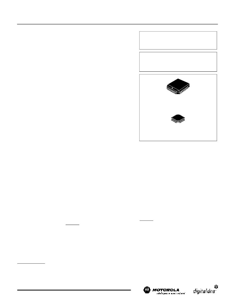
MPC9230
800 MHz LOW VOLTAGE
CLOCK SYNTHESIZER
FA SUFFIX
32-LEAD TQFP PACKAGE
CASE 873A-03
FN SUFFIX
28-LEAD PLCC PACKAGE
CASE 776-02
F
Freescale Semiconductor, Inc.
For More Information On This Product,
Go to: www.freescale.com
n
.
相關PDF資料 |
PDF描述 |
|---|---|
| MPC9350 | LOW VOLTAGE PLL CLOCK DRIVER |
| MPC9350D | LOW VOLTAGE PLL CLOCK DRIVER |
| MPC9446 | 2.5V and 3.3V LVCMOS Clock Fanout Buffer |
| MPC9448 | 3.3V/2.5V LVCMOS 1:12 Clock Fanout Buffer |
| MPC9448D | 3.3V/2.5V LVCMOS 1:12 Clock Fanout Buffer |
相關代理商/技術參數 |
參數描述 |
|---|---|
| MPC9230AC | 功能描述:時鐘合成器/抖動清除器 FSL 800MHz LVPECL Freq. Synthesizer RoHS:否 制造商:Skyworks Solutions, Inc. 輸出端數量: 輸出電平: 最大輸出頻率: 輸入電平: 最大輸入頻率:6.1 GHz 電源電壓-最大:3.3 V 電源電壓-最小:2.7 V 封裝 / 箱體:TSSOP-28 封裝:Reel |
| MPC9230ACR2 | 功能描述:時鐘合成器/抖動清除器 FSL 800MHz LVPECL Freq. Synthesizer RoHS:否 制造商:Skyworks Solutions, Inc. 輸出端數量: 輸出電平: 最大輸出頻率: 輸入電平: 最大輸入頻率:6.1 GHz 電源電壓-最大:3.3 V 電源電壓-最小:2.7 V 封裝 / 箱體:TSSOP-28 封裝:Reel |
| MPC9230EI | 功能描述:時鐘合成器/抖動清除器 FSL 800MHz LVPECL Freq. Synthesizer RoHS:否 制造商:Skyworks Solutions, Inc. 輸出端數量: 輸出電平: 最大輸出頻率: 輸入電平: 最大輸入頻率:6.1 GHz 電源電壓-最大:3.3 V 電源電壓-最小:2.7 V 封裝 / 箱體:TSSOP-28 封裝:Reel |
| MPC9230EIR2 | 功能描述:時鐘合成器/抖動清除器 FSL 800MHz LVPECL Freq. Synthesizer RoHS:否 制造商:Skyworks Solutions, Inc. 輸出端數量: 輸出電平: 最大輸出頻率: 輸入電平: 最大輸入頻率:6.1 GHz 電源電壓-最大:3.3 V 電源電壓-最小:2.7 V 封裝 / 箱體:TSSOP-28 封裝:Reel |
| MPC9230FA | 功能描述:IC PECL CLOCK LV 800MHZ 32-LQFP RoHS:否 類別:集成電路 (IC) >> 時鐘/計時 - 時鐘發生器,PLL,頻率合成器 系列:- 標準包裝:39 系列:- 類型:* PLL:帶旁路 輸入:時鐘 輸出:時鐘 電路數:1 比率 - 輸入:輸出:1:10 差分 - 輸入:輸出:是/是 頻率 - 最大:170MHz 除法器/乘法器:無/無 電源電壓:2.375 V ~ 3.465 V 工作溫度:0°C ~ 70°C 安裝類型:* 封裝/外殼:* 供應商設備封裝:* 包裝:* |
發布緊急采購,3分鐘左右您將得到回復。