- 您現在的位置:買賣IC網 > PDF目錄98034 > MPSH81 (ON SEMICONDUCTOR) Si, PNP, RF SMALL SIGNAL TRANSISTOR, TO-92 PDF資料下載
參數資料
| 型號: | MPSH81 |
| 廠商: | ON SEMICONDUCTOR |
| 元件分類: | 小信號晶體管 |
| 英文描述: | Si, PNP, RF SMALL SIGNAL TRANSISTOR, TO-92 |
| 封裝: | PLASTIC, TO-226AA, 3 PIN |
| 文件頁數: | 5/35頁 |
| 文件大小: | 320K |
| 代理商: | MPSH81 |
第1頁第2頁第3頁第4頁當前第5頁第6頁第7頁第8頁第9頁第10頁第11頁第12頁第13頁第14頁第15頁第16頁第17頁第18頁第19頁第20頁第21頁第22頁第23頁第24頁第25頁第26頁第27頁第28頁第29頁第30頁第31頁第32頁第33頁第34頁第35頁
Surface Mount Information
7–10
Motorola Small–Signal Transistors, FETs and Diodes Device Data
INFORMATION FOR USING SURFACE MOUNT PACKAGES
RECOMMENDED FOOTPRINTS FOR SURFACE MOUNTED APPLICATIONS
Surface mount board layout is a critical portion of the total
design. The footprint for the semiconductor packages must
be the correct size to ensure proper solder connection inter-
face between the board and the package. With the correct
pad geometry, the packages will self align when subjected to
a solder reflow process.
POWER DISSIPATION FOR A SURFACE MOUNT DEVICE
The power dissipation for a surface mount device is a func-
tion of the drain/collector pad size. These can vary from the
minimum pad size for soldering to a pad size given for
maximum power dissipation. Power dissipation for a surface
mount device is determined by TJ(max), the maximum rated
junction temperature of the die, R
θJA, the thermal resistance
from the device junction to ambient, and the operating
temperature, TA. Using the values provided on the data
sheet, PD can be calculated as follows:
PD =
TJ(max) – TA
R
θJA
The values for the equation are found in the maximum
ratings table on the data sheet. Substituting these values into
the equation for an ambient temperature TA of 25°C, one can
calculate the power dissipation of the device. For example,
for a SOT–223 device, PD is calculated as follows.
PD =
150
°C – 25°C
156
°C/W
= 800 milliwatts
The 156
°C/W for the SOT–223 package assumes the use
of the recommended footprint on a glass epoxy printed circuit
board to achieve a power dissipation of 800 milliwatts. There
are other alternatives to achieving higher power dissipation
from the surface mount packages. One is to increase the
area of the drain/collector pad. By increasing the area of the
drain/collector pad, the power dissipation can be increased.
Although the power dissipation can almost be doubled with
this method, area is taken up on the printed circuit board
which can defeat the purpose of using surface mount
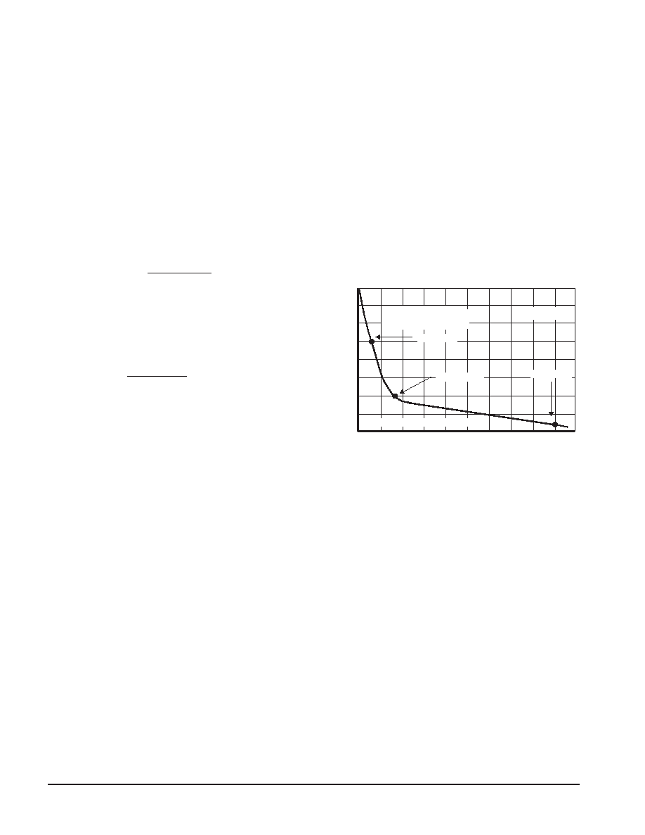
technology. For example, a graph of R
θJA versus drain pad
area is shown in Figure 1.
Another alternative would be to use a ceramic substrate or
an aluminum core board such as Thermal Clad
. Using a
board material such as Thermal Clad, an aluminum core
board, the power dissipation can be doubled using the same
footprint.
T
O
AMBIENT
(
C/W)°
R
JA
,THERMAL
RE
S
IS
TANCE
,J
U
NCTI
O
N
θ
0.8 Watts
1.25 Watts*
1.5 Watts
A, AREA (SQUARE INCHES)
0.0
0.2
0.4
0.6
0.8
1.0
160
140
120
100
80
Board Material = 0.0625
″
G–10/FR–4, 2 oz Copper
TA = 25°C
*Mounted on the DPAK footprint
Figure 1. Thermal Resistance versus Drain Pad
Area for the SOT–223 Package (Typical)
SOLDER STENCIL GUIDELINES
Prior to placing surface mount components onto a printed
circuit board, solder paste must be applied to the pads.
Solder stencils are used to screen the optimum amount.
These stencils are typically 0.008 inches thick and may be
made of brass or stainless steel. For packages such as the
SOT–23, SC–59, SC–70/SOT–323, SC–90/SOT–416,
SOD–123, SOT–223, SOT–363, SO–14, SO–16, and
TSOP–6 packages, the stencil opening should be the same
as the pad size or a 1:1 registration.
相關PDF資料 |
PDF描述 |
|---|---|
| MPSL01ZL1 | 150 mA, 120 V, NPN, Si, SMALL SIGNAL TRANSISTOR, TO-92 |
| MPSL01RLRA | 150 mA, 120 V, NPN, Si, SMALL SIGNAL TRANSISTOR, TO-92 |
| MPSL01RL1 | 150 mA, 120 V, NPN, Si, SMALL SIGNAL TRANSISTOR, TO-92 |
| MPSL01RLRM | 150 mA, 120 V, NPN, Si, SMALL SIGNAL TRANSISTOR, TO-92 |
| MPSL01RLRE | 150 mA, 120 V, NPN, Si, SMALL SIGNAL TRANSISTOR, TO-92 |
相關代理商/技術參數 |
參數描述 |
|---|---|
| MPSH81 D26Z | 制造商:Fairchild Semiconductor Corporation 功能描述:Trans GP BJT PNP 20V 0.05A 3-Pin TO-92 T/R 制造商:Fairchild Semiconductor 功能描述:Trans GP BJT PNP 20V 0.05A 3-Pin TO-92 T/R |
| MPSH81/D75Z | 制造商:Fairchild Semiconductor Corporation 功能描述: |
| MPSH81_D26Z | 功能描述:射頻雙極小信號晶體管 PNP RF Transistor RoHS:否 制造商:NXP Semiconductors 配置:Single 晶體管極性:NPN 最大工作頻率:7000 MHz 集電極—發射極最大電壓 VCEO:15 V 發射極 - 基極電壓 VEBO:2 V 集電極連續電流:0.15 A 功率耗散:1000 mW 直流集電極/Base Gain hfe Min: 最大工作溫度:+ 150 C 封裝 / 箱體:SOT-223 封裝:Reel |
| MPSH81_D27Z | 功能描述:射頻雙極小信號晶體管 PNP RF Transistor RoHS:否 制造商:NXP Semiconductors 配置:Single 晶體管極性:NPN 最大工作頻率:7000 MHz 集電極—發射極最大電壓 VCEO:15 V 發射極 - 基極電壓 VEBO:2 V 集電極連續電流:0.15 A 功率耗散:1000 mW 直流集電極/Base Gain hfe Min: 最大工作溫度:+ 150 C 封裝 / 箱體:SOT-223 封裝:Reel |
| MPSH81_D75Z | 功能描述:射頻雙極小信號晶體管 PNP RF Transistor RoHS:否 制造商:NXP Semiconductors 配置:Single 晶體管極性:NPN 最大工作頻率:7000 MHz 集電極—發射極最大電壓 VCEO:15 V 發射極 - 基極電壓 VEBO:2 V 集電極連續電流:0.15 A 功率耗散:1000 mW 直流集電極/Base Gain hfe Min: 最大工作溫度:+ 150 C 封裝 / 箱體:SOT-223 封裝:Reel |
發布緊急采購,3分鐘左右您將得到回復。