- 您現在的位置:買賣IC網 > PDF目錄361089 > NCN6004AFTBR2 (ON SEMICONDUCTOR) Dual SAM/SIM Interface Integrated Circuit PDF資料下載
參數資料
| 型號: | NCN6004AFTBR2 |
| 廠商: | ON SEMICONDUCTOR |
| 元件分類: | 其它接口 |
| 英文描述: | Dual SAM/SIM Interface Integrated Circuit |
| 中文描述: | SPECIALTY INTERFACE CIRCUIT, PQFP48 |
| 封裝: | PLASTIC, TQFP-48 |
| 文件頁數: | 31/40頁 |
| 文件大小: | 329K |
| 代理商: | NCN6004AFTBR2 |
第1頁第2頁第3頁第4頁第5頁第6頁第7頁第8頁第9頁第10頁第11頁第12頁第13頁第14頁第15頁第16頁第17頁第18頁第19頁第20頁第21頁第22頁第23頁第24頁第25頁第26頁第27頁第28頁第29頁第30頁當前第31頁第32頁第33頁第34頁第35頁第36頁第37頁第38頁第39頁第40頁
NCN6004A
http://onsemi.com
31
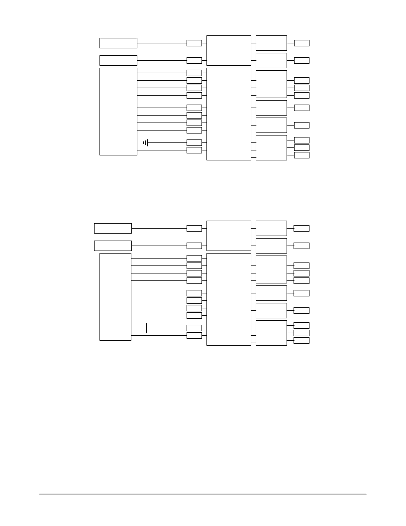
Figure 31. Parallel Operation Wiring
MUX_MODE = Low
13
10
11
12
9
19
16
18
17
15
RESET_A
C4_A
C8_A
I/O_A
CLK_IN_A
I/O_B
C8_B
C4_B
RESET_B
CLK_IN_B
44
5
MUX_MODE
CARD_SEL
BUFFERS
CARD_A
BUFFERS
BUFFER
BUFFER
BUFFER
I/O_A
BUFFER
I/O_B
CARD_B
CLK_A
CLK_B
23
22
21
24
37
38
39
40
30
31
CLOCK GEN.
CLOCK GEN.
MULTIPLEX &
CLOCK DIVIDER
CARD
LOGIC
CONTROL
GND
P
P
C
M
When the chip operates in the parallel mode, all the logic
signals must be independently controlled by the
microcontroller as depicted in Figure 31. The MUX_MODE
pin must be hardwired to VCC and it cannot be changed
during an operation of the chip. Beside this parameter, the
user must select to force or not the internal pull up resistors
as defined by the EN_RPU logic state.
Figure 32. Multiplexed Operation Wiring
MUX_MODE = High
13
10
11
12
9
19
16
18
17
15
RESET_A
C4_A
C8_A
I/O_A
CLK_IN_A
I/O_B
C8_B
C4_B
RESET_B
CLK_IN_B
44
5
MUX_MODE
CARD_SEL
BUFFERS
CARD_A
BUFFERS
BUFFER
BUFFER
BUFFER
I/O_A
BUFFER
I/O_B
CARD_B
CLK_A
CLK_B
23
22
21
24
37
38
39
40
30
31
CLOCK GEN.
CLOCK GEN.
P
P
C
M
MULTIPLEX &
CLOCK DIVIDER
CARD
LOGIC
CONTROL
VCC
In the multiplexed mode, the microprocessor CARD_B
side pins are not connected, the logic signals and the I/O line
being shared with CARD_A associated with the CRD_SEL
control bit: Figure 32. A key point is to make sure there is no
connection associated with the I/O_B pin since this pin is
internally shared with the I/O line transaction. The
CLK_IN_A and CLK_IN_B signals are independent and
can be routed to any of the card thanks to the built-in clock
multiplexer.
DATA I/O LEVEL SHIFTER
The built in structure provides a level shifter on each card
output signals, the I/O line being driven differently as
depicted in Figure 33. Since the NCN6004A can operate in
either a multiplexed or parallel mode, provisions have been
made to route the I/O_A input pin to either CARD_A or
CARD_B.
In both case, the I/O pins are driven by an open drain
structure with a 20 k pull up resistor as shown Figure 33.
To achieve the 0.80 s maximum rise time requested by the
EMV specifications, an accelerator circuit is added on both
side of each I/O line. These pulsed circuits yield boost
current to charge the stray capacitance, thus accelerating the
positive going slope of the I/O signal. On the other hand, the
active pull down NMOS device Q5 provides a low
impedance to ground during the battery up and DC/DC
start-up phase, avoiding any uncontrolled voltage spikes on
the I/O lines.
相關PDF資料 |
PDF描述 |
|---|---|
| NCN6004A | Dual SAM/SIM Interface Integrated Circuit |
| NCN6010DTBR2 | SIM Card Supply and Level Shifter |
| NCN6010 | SIM Card Supply and Level Shifter |
| NCN6010D | SIM Card Supply and Level Shifter |
| NCN6010DTB | SIM Card Supply and Level Shifter |
相關代理商/技術參數 |
參數描述 |
|---|---|
| NCN6004AFTBR2G | 功能描述:輸入/輸出控制器接口集成電路 2.7V POS/ATM Smart Card Interface RoHS:否 制造商:Silicon Labs 產品: 輸入/輸出端數量: 工作電源電壓: 最大工作溫度:+ 85 C 最小工作溫度:- 40 C 安裝風格:SMD/SMT 封裝 / 箱體:QFN-64 封裝:Tray |
| NCN6010 | 制造商:ONSEMI 制造商全稱:ON Semiconductor 功能描述:SIM Card Supply and Level Shifter |
| NCN6010/D | 制造商:ONSEMI 制造商全稱:ON Semiconductor 功能描述:SIM Card Supply and Level Shifter |
| NCN6010_06 | 制造商:ONSEMI 制造商全稱:ON Semiconductor 功能描述:SIM Card Supply and Level Shifter |
| NCN6010D | 制造商:ONSEMI 制造商全稱:ON Semiconductor 功能描述:SIM Card Supply and Level Shifter |
發布緊急采購,3分鐘左右您將得到回復。