- 您現在的位置:買賣IC網 > PDF目錄361091 > NCP1406SNT1 (ON SEMICONDUCTOR) 25 V/25 mA PFM Step−Up DC−DC Converter PDF資料下載
參數資料
| 型號: | NCP1406SNT1 |
| 廠商: | ON SEMICONDUCTOR |
| 元件分類: | 穩壓器 |
| 英文描述: | 25 V/25 mA PFM Step−Up DC−DC Converter |
| 中文描述: | 1.5 A SWITCHING REGULATOR, 1000 kHz SWITCHING FREQ-MAX, PDSO5 |
| 封裝: | SC-59, SOT-23, TSOP-5 |
| 文件頁數: | 16/23頁 |
| 文件大小: | 224K |
| 代理商: | NCP1406SNT1 |
NCP1406
http://onsemi.com
16
PCB Layout Guidelines
PCB layout is very important for switching converter
performance. All the converter’s external components
should be placed closed to the IC. The schematic, PCB
trace layout, and component placement of the stepup
DCDC converter demonstration board are shown in
Figure 46 to Figure 49 for PCB layout design reference.
The following guidelines should be observed:
1. Grounding
Singlepoint grounding should be used for the output
power return ground, the input power return ground, and
the device switch ground to reduce noise. The input ground
and output ground traces must be thick and short enough for
current to flow through. A ground plane should be used to
reduce ground bounce.
2. Power Traces
Low resistance conducting paths (short and thick traces)
should be used for the power carrying traces to reduce
power loss so as to improve efficiency (short and thick
traces for connecting the inductor L can also reduce stray
inductance). The path between C1, L1, D1, and C2 should
be kept short. The trace from L to LX pin of the IC should
also be kept short.
3.
External Feedback Components
Feedback resistors R1 and R2, and feedforward
capacitor C3 should be located as close to the FB pin as
possible to minimize noise picked up by the FB pin. The
ground connection of the feedback resistor divider should
be connected directly to the GND pin.
4. Input Capacitor
The input capacitor should be located close to both the
input to the inductor and the VDD pin of the IC.
5. Output Capacitor
The output capacitor should be placed close to the
output terminals to obtain better smoothing effect on output
ripple voltage.
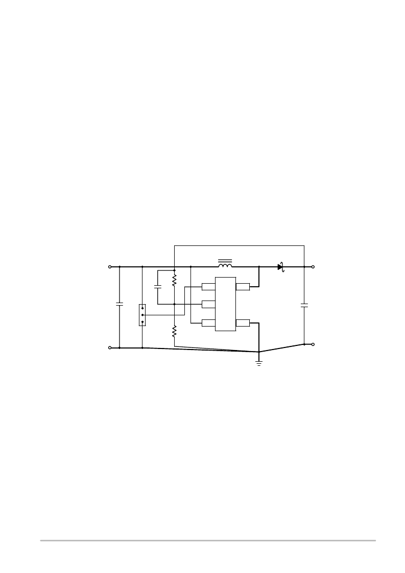
V
IN
1.8 V to 5.0 V
C
1
10 F
3
VDD
2
FB
1
CE
5
LX
4
GND
N
L1 8.2 H
D1
MBR0530T1
C
2
3.3 F
Figure 46. StepUp Converter Demonstration Board Schematic
TP1
C3
R1
Enable
R2
V
OUT
25 V
TP3
TP2
GND
TP4
GND
相關PDF資料 |
PDF描述 |
|---|---|
| NCP1406SNT1G | 25 V/25 mA PFM Step−Up DC−DC Converter |
| NCP1410DMR2 | 250 mA Sync-Rect PFM Step-Up DC-DC Converter with Low-Battery Detector |
| NCP1410 | 250 mA Sync-Rect PFM Step-Up DC-DC Converter with Low-Battery Detector |
| NCP1411DMR2 | Sync-Rect PFM Step-Up DC-DC Converter with Low-Battery Detector and Ring-Killer |
| NCP1411D | Sync-Rect PFM Step-Up DC-DC Converter with Low-Battery Detector and Ring-Killer |
相關代理商/技術參數 |
參數描述 |
|---|---|
| NCP1406SNT1G | 功能描述:直流/直流開關轉換器 25V 25mA Boost PFM RoHS:否 制造商:STMicroelectronics 最大輸入電壓:4.5 V 開關頻率:1.5 MHz 輸出電壓:4.6 V 輸出電流:250 mA 輸出端數量:2 最大工作溫度:+ 85 C 安裝風格:SMD/SMT |
| NCP1406V15GEVB | 功能描述:電源管理IC開發工具 NCP1406 EVAL BRD RoHS:否 制造商:Maxim Integrated 產品:Evaluation Kits 類型:Battery Management 工具用于評估:MAX17710GB 輸入電壓: 輸出電壓:1.8 V |
| NCP1406V25GEVB | 功能描述:電源管理IC開發工具 NCP1406 EVAL BRD RoHS:否 制造商:Maxim Integrated 產品:Evaluation Kits 類型:Battery Management 工具用于評估:MAX17710GB 輸入電壓: 輸出電壓:1.8 V |
| NCP1410DMR2 | 功能描述:直流/直流開關轉換器 ANA DC-DC CONVERTER RoHS:否 制造商:STMicroelectronics 最大輸入電壓:4.5 V 開關頻率:1.5 MHz 輸出電壓:4.6 V 輸出電流:250 mA 輸出端數量:2 最大工作溫度:+ 85 C 安裝風格:SMD/SMT |
| NCP1410DMR2G | 功能描述:直流/直流開關轉換器 ANA DC-DC CONVERTER RoHS:否 制造商:STMicroelectronics 最大輸入電壓:4.5 V 開關頻率:1.5 MHz 輸出電壓:4.6 V 輸出電流:250 mA 輸出端數量:2 最大工作溫度:+ 85 C 安裝風格:SMD/SMT |
發布緊急采購,3分鐘左右您將得到回復。