- 您現(xiàn)在的位置:買(mǎi)賣(mài)IC網(wǎng) > Datasheet目錄45 > NIS5112D1R2G (ON Semiconductor)IC ELECTRONIC FUSE HOTSWAP 8SOIC Datasheet資料下載
參數(shù)資料
| 型號(hào): | NIS5112D1R2G |
| 廠商: | ON Semiconductor |
| 文件頁(yè)數(shù): | 2/9頁(yè) |
| 文件大小: | 410K |
| 描述: | IC ELECTRONIC FUSE HOTSWAP 8SOIC |
| 標(biāo)準(zhǔn)包裝: | 1 |
| 功能: | 電子保險(xiǎn)絲 |
| 輸入電壓: | 9 V ~ 18 V |
| 電流 - 輸出: | 2A |
| 工作溫度: | -40°C ~ 175°C |
| 安裝類型: | 表面貼裝 |
| 封裝/外殼: | 8-SOIC(0.154",3.90mm 寬) |
| 供應(yīng)商設(shè)備封裝: | 8-SOICN |
| 包裝: | 剪切帶 (CT) |
| 其它名稱: | NIS5112D1R2GOSCT |
NIS5112
http://onsemi.com
2
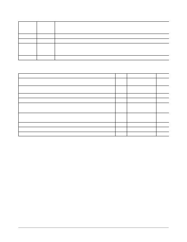
Table 1. FUNCTIONAL PIN DESCRIPTION
Pin
Function
Description
3
Enable/Timer
A high level signal on this pin allows the device to begin operation. Connection of a capacitor will delay
turn on for timing purposes. A low input signal inhibits the operation.
1
Ground
Negative input voltage to the device. This is used as the internal reference for the IC.
4
I
Limit
A resistor between this pin and the source pin sets the current limit level.
5,6,7
Source
Source of power FET, which is also the switching node for the load.
2
dV/dt
A capacitor from this pin to ground programs the slew rate of the output at turn on. This capacitor is
discharged by an internal discharge circuit when the device is disabled via the enable pin.
8
V
CC
Positive input voltage to the device.
Table 2. MAXIMUM RATINGS (Maximum ratings are those, that, if exceeded, may cause damage to the device. Electrical
characteristics are not guaranteed over this range)
Rating
Symbol
Value
Unit
Input Voltage, Operating,
SteadyState (Input+ to Input)
Transient (Conditions 1 ms)
V
in
0.3 to 18
0.3 to 25
V
Drain Voltage, Operating,
SteadyState (Drain to Input)
Transient (Conditions 1 ms)
V
DD
0.3 to 18
0.3 to 25
V
Drain Current, Peak (Internally Clamped)
I
Dpk
25
A
Drain Current, Continuous (T
A
=25癈), (Note 2)
I
Davg
5.3
A
Thermal Resistance, JunctiontoAir
0.5 in
2
Copper
1.0 in
2
Copper
Q
JA
120
110
癈/W
癈/W
Thermal Resistance, JunctiontoLead (Pin 8)
Q
JL
27
癈/W
Power Dissipation (T
A
= 25癈) (Note 1)
P
max
1.0
W
Operating Temperature Range (Note 2)
T
J
40 to 175
癈
Nonoperating Temperature Range
T
J
55 to 175
癈
Lead Temperature, Soldering (10 Sec)
T
L
260
癈
Stresses exceeding Maximum Ratings may damage the device. Maximum Ratings are stress ratings only. Functional operation above the
Recommended Operating Conditions is not implied. Extended exposure to stresses above the Recommended Operating Conditions may affect
device reliability.
1. Mounted on FR4 board, 1 in sq pad, 1 oz coverage.
2. Actual maximum junction temperature is limited by an internal protection circuit and will not reach the absolute maximum temperature as
specified.
相關(guān)PDF資料 |
PDF描述 |
|---|---|
| NIS5132MN2TXG | IC ELECTRONIC FUSE 12V 10DFN |
| NIS5132MN3TXG | IC ELECTRONIC FUSE 12V 10-DFN |
| NSI45015WT1G | IC LED DRIVER LINEAR SOD-123 |
| NSI45020AT1G | IC LED DRIVER LINEAR SOD-123 |
| NSI45020JZT1G | IC LED DRVR CONST CURRENT SOT223 |
相關(guān)代理商/技術(shù)參數(shù) |
參數(shù)描述 |
|---|---|
| NIS5112D2R2G | 功能描述:熱插拔功率分布 PM ELCTRNC FUSE IN SO8 RoHS:否 制造商:Texas Instruments 產(chǎn)品:Controllers & Switches 電流限制: 電源電壓-最大:7 V 電源電壓-最小:- 0.3 V 工作溫度范圍: 功率耗散: 安裝風(fēng)格:SMD/SMT 封裝 / 箱體:MSOP-8 封裝:Tube |
| NIS5112D2R2G-CUT TAPE | 制造商:ON 功能描述:NIS Series 12 V 92 uA Surface Mount Electronic Fuse - SOIC-8 |
| NIS5131 | 制造商:ONSEMI 制造商全稱:ON Semiconductor 功能描述:Low cap. diode array for 2 Line High Speed USB protection devic |
| NIS5132 | 制造商:ONSEMI 制造商全稱:ON Semiconductor 功能描述:12 Volt Electronic Fuse,3.6 AMP, 12 VOLT ELECTRONIC FUSE |
| NIS5132-35GEVB | 功能描述:BOARD EVAL ELECT FUSE NIS5132-35 RoHS:是 類別:編程器,開(kāi)發(fā)系統(tǒng) >> 評(píng)估演示板和套件 系列:- 標(biāo)準(zhǔn)包裝:1 系列:PCI Express® (PCIe) 主要目的:接口,收發(fā)器,PCI Express 嵌入式:- 已用 IC / 零件:DS80PCI800 主要屬性:- 次要屬性:- 已供物品:板 |
發(fā)布緊急采購(gòu),3分鐘左右您將得到回復(fù)。