- 您現在的位置:買賣IC網 > Datasheet目錄45 > NIS5112D1R2G (ON Semiconductor)IC ELECTRONIC FUSE HOTSWAP 8SOIC Datasheet資料下載
參數資料
| 型號: | NIS5112D1R2G |
| 廠商: | ON Semiconductor |
| 文件頁數: | 7/9頁 |
| 文件大小: | 410K |
| 描述: | IC ELECTRONIC FUSE HOTSWAP 8SOIC |
| 標準包裝: | 1 |
| 功能: | 電子保險絲 |
| 輸入電壓: | 9 V ~ 18 V |
| 電流 - 輸出: | 2A |
| 工作溫度: | -40°C ~ 175°C |
| 安裝類型: | 表面貼裝 |
| 封裝/外殼: | 8-SOIC(0.154",3.90mm 寬) |
| 供應商設備封裝: | 8-SOICN |
| 包裝: | 剪切帶 (CT) |
| 其它名稱: | NIS5112D1R2GOSCT |
NIS5112
http://onsemi.com
7
DEVICE OPERATION
Basic Operation
This device is a selfprotected, resettable, electronic fuse.
It contains circuits to monitor the input voltage, output
current, die temperature, turnon di/dt and turnon dV/dt, as
well as an enable/timer function.
On application of the input voltage, the device will apply
the input voltage to the load based on the restrictions of the
controlling circuits. The dV/dt of the output voltage can be
programmed by the addition of a capacitor to the dV/dt pin,
or if left open, the output current will be limited by the
internally controlled di/dt.
The device will remain on as long as the temperature does
not exceed the 135癈 limit that is programmed into the chip.
The current limit circuit does not shut down the part but will
reduce the conductivity of the FET to maintain a constant
current as long as it remains at the set level. The input
overvoltage clamp also does not shut down the part, but will
limit the output voltage to 15 V in the event that the input
exceeds that level.
The device can be turned on and off by the enable/timer
function, which can also be used to reset the device after a
thermal fault if the thermal latch version is chosen.
An internal charge pump provides bias for the gate voltage
of the internal Nchannel power FET and also for the current
limit circuit. The remainder of the control circuitry operates
between the input voltage (V
CC
) and ground.
dV/dt
This circuit is comprised of an operational amplifier and
current source as shown in Figure 9. The enable circuit
controls a FET that keeps the slewrate capacitor discharged
any time the device is disabled. When the enable pin is
released (lowtohigh transition) or when power is applied
with the enable pin in a high state, the dV/dt capacitor begins
to charge due to the 80 mA in the current source. The
amplifier controls the output voltage and tracks the voltage
on the dV/dt cap scaled by a factor of 2. The output voltage
will continue to ramp higher until it reaches the input
voltage, or until the 15 V clamp limits it.
The equation for the output slew rate is
dV/dt = (I/C
dV/dt
) x 2.
Where:
I is 80 mA (internal current source)
C
dV/dt
is the desired dV/dt capacitor value.
The dV/dt ramp begins with a small step of about 200 mV.
This step causes a current surge into the output load
capacitance which can be seen in Figure 6. The peak level
of this surge will be limited to the overload level of the
current limit.
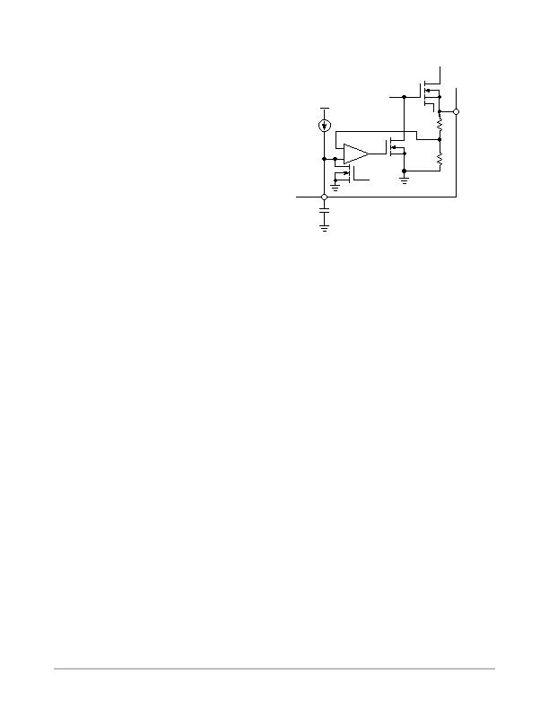
Figure 9. dV/dt Circuit
+
Enable
Source
dV/dt
R
R
80 mA
Overvoltage Clamp
The overvoltage clamp consists of an amplifier and
reference. It monitors the output voltage and if the output
voltage exceeds 15 V, the gate drive of the main FET is
reduced to limit the output. This is intended to allow
operation through transients while protecting the load. If an
overvoltage condition exists for many seconds, the device
may overheat due to the voltage drop across the FET
combined with the load current. In this event, the thermal
protection circuit would shut down the device.
Enable/Timer
The enable/timer pin can function either as a direct enable
pin, or as a time delay. In the enable mode, an open collector
device is connected to this pin. When the device is in its low
impedance mode, this pin is low and the operation of the chip
is disabled. If a time delay is required, a capacitor is added
to this pin.
If a capacitor is added without an open collector device,
the turn on will be delayed from the time at which the UVLO
voltage is reached. If an open collector device is also used,
the delay will start from the time that it goes into its high
impedance state. The capacitor is charged by an internal
current source of 80 mA (typical).
The nominal trip voltage of the comparator is 2.5 V and
was designed to be compatible with most logic families. In
general, logic gates can be tied directly to this pin, but it is
recommended that this be tested.
相關PDF資料 |
PDF描述 |
|---|---|
| NIS5132MN2TXG | IC ELECTRONIC FUSE 12V 10DFN |
| NIS5132MN3TXG | IC ELECTRONIC FUSE 12V 10-DFN |
| NSI45015WT1G | IC LED DRIVER LINEAR SOD-123 |
| NSI45020AT1G | IC LED DRIVER LINEAR SOD-123 |
| NSI45020JZT1G | IC LED DRVR CONST CURRENT SOT223 |
相關代理商/技術參數 |
參數描述 |
|---|---|
| NIS5112D2R2G | 功能描述:熱插拔功率分布 PM ELCTRNC FUSE IN SO8 RoHS:否 制造商:Texas Instruments 產品:Controllers & Switches 電流限制: 電源電壓-最大:7 V 電源電壓-最小:- 0.3 V 工作溫度范圍: 功率耗散: 安裝風格:SMD/SMT 封裝 / 箱體:MSOP-8 封裝:Tube |
| NIS5112D2R2G-CUT TAPE | 制造商:ON 功能描述:NIS Series 12 V 92 uA Surface Mount Electronic Fuse - SOIC-8 |
| NIS5131 | 制造商:ONSEMI 制造商全稱:ON Semiconductor 功能描述:Low cap. diode array for 2 Line High Speed USB protection devic |
| NIS5132 | 制造商:ONSEMI 制造商全稱:ON Semiconductor 功能描述:12 Volt Electronic Fuse,3.6 AMP, 12 VOLT ELECTRONIC FUSE |
| NIS5132-35GEVB | 功能描述:BOARD EVAL ELECT FUSE NIS5132-35 RoHS:是 類別:編程器,開發系統 >> 評估演示板和套件 系列:- 標準包裝:1 系列:PCI Express® (PCIe) 主要目的:接口,收發器,PCI Express 嵌入式:- 已用 IC / 零件:DS80PCI800 主要屬性:- 次要屬性:- 已供物品:板 |
發布緊急采購,3分鐘左右您將得到回復。