- 您現(xiàn)在的位置:買賣IC網(wǎng) > PDF目錄361005 > PLSI1016-80LT Electrically-Erasable Complex PLD PDF資料下載
參數(shù)資料
| 型號: | PLSI1016-80LT |
| 英文描述: | Electrically-Erasable Complex PLD |
| 中文描述: | 電可擦除復(fù)雜可編程邏輯器件 |
| 文件頁數(shù): | 2/12頁 |
| 文件大小: | 120K |
| 代理商: | PLSI1016-80LT |
Specifications
ispLSI 1048
2
USEispLS 1048EAFORNEW
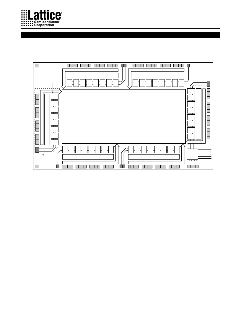
Eight GLBs, 16 I/O cells, two dedicated inputs (one
dedicated input in Megablock B and E) and one ORP are
connected together to make a Megablock (see figure 1).
The outputs of the eight GLBs are connected to a set of
16 universal I/O cells by the ORP. The ispLSI 1048
device contains six of these Megablocks.
COMMERCAL&INDUSTRAL
GLBs and I/O cells. The Clock Distribution Network can
also be driven from a special clock GLB (D0 on the
ispLSI 1048 device). The logic of this GLB allows the user
to create an internal clock from a combination of internal
signals within the device.
DESGNS
GLBs. Delays through the GRP have been equalized to
minimize timing skew.
The device also has 96 I/O cells, each of which is directly
connected to an I/O pin. Each I/O cell can be individually
programmed to be a combinatorial input, registered in-
put, latched input, output or bi-directional
I/O pin with 3-state control. Additionally, all outputs are
polarity selectable, active high or active low. The signal
levels are TTL compatible voltages and the output drivers
can source 4 mA or sink 8 mA.
The GRP has as its inputs the outputs from all of the GLBs
and all of the inputs from the bi-directional I/O cells. All of
these signals are made available to the inputs of the
Clocks in the ispLSI 1048 device are selected using the
Clock Distribution Network. Four dedicated clockpins
(Y0, Y1, Y2 and Y3) are brought into the distribution
network, and five clock outputs (CLK 0, CLK 1, CLK 2,
IOCLK 0 and IOCLK 1) are provided to route clocks to the
Functional Block Diagram
Figure 1. ispLSI 1048 Functional Block Diagram
Output Routing Pool (ORP)
B0
B1
B2
B3
B4
B5
B6
B7
Output Routing Pool (ORP)
C0
C1
C2
C3
C4
C5
C6
C7
Output Routing Pool (ORP)
F7
F6
F5
F4
F3
F2
F1
F0
Input Bus
Output Routing Pool (ORP)
E7
E6
E5
E4
E3
E2
E1
E0
Input Bus
A0
A1
A2
A3
A4
A5
A6
A7
Logic Blocks
(GLBs)
Megablock
I
Global
Routing
Pool
(GRP)
CLK 0
CLK 1
CLK 2
IOCLK 0
IOCLK 1
Clock
Distribution
Network
D7
D6
D5
D4
D3
D2
D1
D0
O
I/O
94
I/O
95
I/O
93
I/O
92
I/O
91
I/O
90
I/O
89
I/O
88
I/O
87
I/O
86
I/O
85
I/O
84
I/O
83
I/O
82
I/O
81
I/O
80
IN
11
I/O
78
I/O
79
I/O
77
I/O
76
I/O
75
I/O
74
I/O
73
I/O
72
I/O
71
I/O
70
I/O
69
I/O
68
I/O
67
I/O
66
I/O
65
I/O
64
IN
8
IN
10
I/O
17
I/O
16
I/O
18
I/O
19
I/O
20
I/O
21
I/O
22
I/O
23
I/O
24
I/O
25
I/O
26
I/O
27
I/O
28
I/O
29
I/O
30
I/O
31
SDO/
IN3
Y
0
Y
1
Y
2
Y
3
I/O
33
I/O
32
I/O
34
I/O
35
I/O
36
I/O
37
I/O
38
I/O
39
I/O
40
I/O
41
I/O
42
I/O
43
I/O
44
I/O
45
I/O
46
I/O
47
SCLK/
IN 5
IN
4
IN 7
IN 6
I/O 6
I/O 6
I/O 6
I/O 6
I/O 5
I/O 5
I/O 5
I/O 5
I/O 5
I/O 5
I/O 5
I/O 5
I/O 5
I/O 5
I/O 4
I/O 4
I/O 0
I/O 1
I/O 2
I/O 3
I/O 6
I/O 7
I/O 8
I/O 9
I/O 10
I/O 11
I/O 12
I/O 13
I/O 14
I/O 15
SDI/IN 0
MODE/IN 1
I/O 4
I/O 5
ispEN
RESET
Input Bus
Input Bus
l
0139F(1)-48-isp
相關(guān)PDF資料 |
PDF描述 |
|---|---|
| PLSI1016-90LT | Low Glitch 16-Bit Voltage Output DAC; Package: PDIP; No of Pins: 16; Temperature Range: 0°C to +70°C |
| PLSI1016E100LJ | Low Glitch 16-Bit Voltage Output DAC; Package: SO; No of Pins: 16; Temperature Range: -40°C to +85°C |
| PLSI1016E125LJ | 16-Bit Rail-to-Rail Micropower DACs in SO-8 Package; Package: PDIP; No of Pins: 8; Temperature Range: -40°C to +85°C |
| PLSI1016E-80LJ | Electrically-Erasable Complex PLD |
| ISRT44080 | |
相關(guān)代理商/技術(shù)參數(shù) |
參數(shù)描述 |
|---|---|
| PLSI1016-80LT44 | 制造商:未知廠家 制造商全稱:未知廠家 功能描述:Electrically-Erasable Complex PLD |
| PLSI1016-90LJ | 制造商:未知廠家 制造商全稱:未知廠家 功能描述:Electrically-Erasable Complex PLD |
| PLSI1016-90LT | 制造商:未知廠家 制造商全稱:未知廠家 功能描述:Electrically-Erasable Complex PLD |
| PLSI1016-90LT44 | 制造商:未知廠家 制造商全稱:未知廠家 功能描述:Electrically-Erasable Complex PLD |
| PLSI1016E100LJ | 制造商:LATTICE 制造商全稱:Lattice Semiconductor 功能描述:High-Density Programmable Logic |
發(fā)布緊急采購,3分鐘左右您將得到回復(fù)。