- 您現在的位置:買賣IC網 > Datasheet目錄46 > SC427MLTRT (Semtech)IC REG DL BUCK/LINEAR 32MLPQ Datasheet資料下載
參數資料
| 型號: | SC427MLTRT |
| 廠商: | Semtech |
| 文件頁數: | 29/33頁 |
| 文件大小: | 894K |
| 描述: | IC REG DL BUCK/LINEAR 32MLPQ |
| 標準包裝: | 1 |
| 系列: | EcoSpeed®, SmartDrive™ |
| 拓撲: | 降壓(降壓)(1),線性(LDO)(1) |
| 功能: | 任何功能 |
| 輸出數: | 2 |
| 頻率 - 開關: | 1MHz |
| 電壓/電流 - 輸出 1: | 可調,10A |
| 電壓/電流 - 輸出 2: | 5V,200mA |
| 帶 LED 驅動器: | 無 |
| 帶監控器: | 無 |
| 帶序列發生器: | 無 |
| 電源電壓: | 3 V ~ 28 V |
| 工作溫度: | -40°C ~ 85°C |
| 安裝類型: | 表面貼裝 |
| 封裝/外殼: | 32-VFQFN 裸露焊盤 |
| 供應商設備封裝: | 32-MLPQ(5x5) |
| 包裝: | 標準包裝 |
| 其它名稱: | SC427MLDKR |
第1頁第2頁第3頁第4頁第5頁第6頁第7頁第8頁第9頁第10頁第11頁第12頁第13頁第14頁第15頁第16頁第17頁第18頁第19頁第20頁第21頁第22頁第23頁第24頁第25頁第26頁第27頁第28頁當前第29頁第30頁第31頁第32頁第33頁
SC417/SC427
29
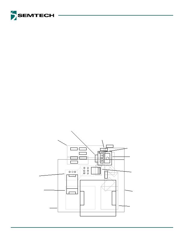
PCB Layout Guidelines
The optimum layout for the SC417/SC427 is shown in
Figure 15. This layout shows an integrated FET buck regu-
lator with a maximum current of 10A. The total PCB area is
approximately 20 x 25 mm.
Critical Layout Guidelines
The following critical layout guidelines must be followed
to ensure proper performance of the device.
IC Decoupling capacitors
PGND plane
AGND island
FB, VOUT, and other analog control signals
BST, ILIM, and LX
CIN and COUT placement and Current Loops
IC Decoupling Capacitors
A 0.1 糉 capacitor must be located as close as
possible to the IC and directly connected to pins
3 (V5V) and 4 (AGND).
All other decoupling capacitors must be located
as close as possible to the IC.
"
"
"
"
"
"
"
"
PGND Plane
PGND requires its own copper plane with no
other signal traces routed on it.
Copper planes, multiple vias and wide traces are
needed to connect PGND to input capacitors,
output capacitors, and the PGND pins on the IC.
The PGND copper area between the input
capacitors, output capacitors and PGND pins
must be as tight and compact as possible to
reduce the area of the PCB that is exposed to
noise due to current flow on this node.
Connect PGND to AGND with a short trace or
0& resistor. This connection should be as close
to the IC as possible.
AGND Island
AGND should have its own island of copper with
no other signal traces routed on this layer that
connects the AGND pins and pad of the IC to the
analog control components.
All of the components for the analog control cir-
cuitry should be located so that the connections
"
"
"
"
"
"
Applications Information (continued)
VOUT Plane
on Top layer
L
CLDO
C
IN
CFF
RFB2
RFB1
RILIM
RLDO2
RLDO1
LX plane on inner
or bottom layer
All components
shown Top Side
AGND plane on
inner layer
V
IN
plane on inner
or bottom layer
RGND AGND connects to
PGND close to SC417/SC427
Pin 1 marking
SC417/SC427
with vias for LX,
AGND, VIN
C
OUT
PGND on inner
or bottom layer
PGND
PGND on
Top Layer
V5V Decoupling Capacitor
Figure 15 PCB Layout
相關PDF資料 |
PDF描述 |
|---|---|
| SE95D,112 | IC SENSOR TEMP 2.8-5.5V SOT96-1 |
| SE97BTP,547 | IC TEMP SENSOR DIMM 8HWSON |
| SE98ATP,547 | IC TEMP SENSOR DDR 8-HWSON |
| SG6901ASZ | IC PFC CTLR AVERAGE CURR 20SOIC |
| SG6932SZ | IC PFC CONTROLLER CCM 16SOP |
相關代理商/技術參數 |
參數描述 |
|---|---|
| SC428 | 制造商:Mallory 功能描述:Sonalert |
| SC4-28 | 功能描述:SCREW 4-40 HEX .5"L FOR CONN MNT RoHS:是 類別:盒,外殼,支架 >> 卡架 - 配件 系列:VectorPak™ 標準包裝:1 系列:VectorPak™ 附件類型:EFP 模塊 適用于相關產品:PCB |
| SC428312CFGE | 制造商:Freescale Semiconductor 功能描述: |
| SC42920FNR2 | 制造商:Motorola Inc 功能描述: |
| SC430769CFNER | 制造商:Freescale Semiconductor 功能描述:SMOKE DETECTOR |
發布緊急采購,3分鐘左右您將得到回復。