- 您現(xiàn)在的位置:買(mǎi)賣(mài)IC網(wǎng) > PDF目錄98215 > TFP510PAPG4 (TEXAS INSTRUMENTS INC) SPECIALTY CONSUMER CIRCUIT, PQFP64 PDF資料下載
參數(shù)資料
| 型號(hào): | TFP510PAPG4 |
| 廠商: | TEXAS INSTRUMENTS INC |
| 元件分類(lèi): | 消費(fèi)家電 |
| 英文描述: | SPECIALTY CONSUMER CIRCUIT, PQFP64 |
| 封裝: | 10 X 10 MM, 1 MM HEIGHT, 0.50 MM PITCH, GREEN, PLASTIC, HTQFP-64 |
| 文件頁(yè)數(shù): | 2/27頁(yè) |
| 文件大小: | 383K |
| 代理商: | TFP510PAPG4 |
第1頁(yè)當(dāng)前第2頁(yè)第3頁(yè)第4頁(yè)第5頁(yè)第6頁(yè)第7頁(yè)第8頁(yè)第9頁(yè)第10頁(yè)第11頁(yè)第12頁(yè)第13頁(yè)第14頁(yè)第15頁(yè)第16頁(yè)第17頁(yè)第18頁(yè)第19頁(yè)第20頁(yè)第21頁(yè)第22頁(yè)第23頁(yè)第24頁(yè)第25頁(yè)第26頁(yè)第27頁(yè)
TFP510
TI PanelBus DIGITAL TRANSMITTER
SLDS146B JANUARY 2002 REVISED DECEMBER 2002
10
POST OFFICE BOX 655303
DALLAS, TEXAS 75265
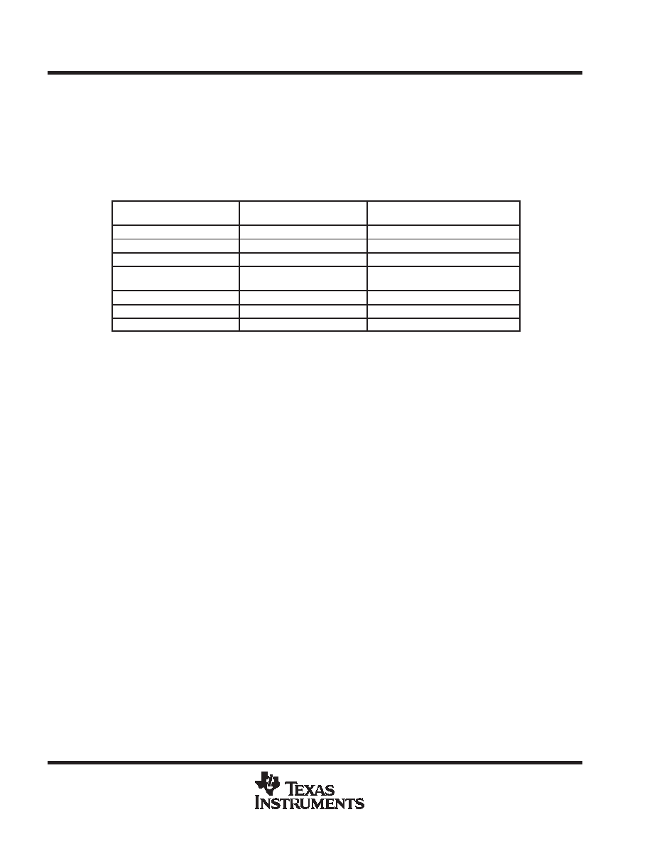
T.M.D.S. pixel data and control signal encoding
For T.M.D.S., only one of two possible T.M.D.S. characters for a given pixel is transmitted at a given time. The
transmitter keeps a running count of the number of ones and zeros previously sent and transmits the character
that minimizes the number of transitions and approximate a dc balance of the transmission line. Three T.M.D.S.
channels are used to transmit RGB pixel data during the active video interval (DE = high). These same three
channels are also used to transmit HSYNC, VSYNC, and three control signals, CTL[3:1], during the inactive
display or blanking interval (DE = low). The following table maps the transmitted output data to the appropriate
T.M.D.S. output channel in a DVI-compliant system.
INPUT PINS
(VALID FOR DE = high)
T.M.D.S. OUTPUT CHANNEL
TRANSMITTED PIXEL DATA
ACTIVE DISPLAY (DE = high)
DATA[23:16]
Channel 2 (TX2
±)
Red[7:0]
DATA[15:8]
Channel 1 (TX1
±)
Green[7:0]
DATA[7:0]
Channel 0 (TX0
±)
Blue[7:0]
INPUT PINS
(VALID FOR DE = low)
T.M.D.S. OUTPUT CHANNEL
TRANSMITTED CONTROL DATA
BLANKING INTERVAL (DE = low)
CTL3, CTL2 (see Note 8)
Channel 2 (TX2
±)
CTL[3:2]
CTL1 (see Note 8)
Channel 1 (TX1
±)
CTL[1]
HSYNC, VSYNC
Channel 0 (TX0
±)
HSYNC, VSYNC
NOTE 8: The TFP510 encodes and transfers the CTL[3:1] inputs during the vertical blanking interval. The
TFP510 internally generates CTL3 for HDCP operation and the CTL[2:1] inputs are reserved for
future use. When DE = high, the CTL and SYNC pins must be held constant.
universal graphics controller interface voltage signal levels
The universal graphics controller interface can operate in the following two distinct voltage modes:
D The high-swing mode where standard 3.3-V CMOS signaling levels are used
D The low-swing mode where adjustable 1.1-V to 1.8-V signaling levels are used
To select the high-swing mode, the VREF input pin must be tied to the 3.3-V power supply.
To select the low-swing mode, the VREF input must be = 0.55 to 0.9 V.
In the low-swing mode, VREF is used to set the midpoint of the adjustable signaling levels. The allowable range
of values for VREF is from 0.55 V to 0.9 V. The typical approach is to provide VREF to the chip using a simple
voltage-divider circuit. The minimum allowable input signal swing in the low-swing mode is VREF ± 0.2 V. In
low-swing mode, the VREF input is common to all differential input receivers.
universal graphics controller interface clock inputs
The universal graphics controller interface of the TFP510 supports both single-ended and fully differential clock
input modes. In the differential clock input mode, the universal graphics controller interface uses the crossover
point between the IDCK+ and IDCK signals as the timing reference for latching incoming data (DATA[23:0],
DE, HSYNC, and VSYNC). Differential clock inputs provide greater common-mode noise rejection. The
differential clock input mode is only available in the low-swing mode. In the single-ended clock input mode, the
IDCK+ input (pin 57) should be connected to the single-ended clock source and the IDCK input (pin 56) should
be tied to GND.
The universal graphics controller interface of the TFP510 provides selectable 12-bit, dual-edge and 24-bit,
single-edge input clocking modes. In the 12-bit dual-edge mode, the 12-bit data is latched on each edge of the
input clock. In the 24-bit single-edge mode, the 24-bit data is latched on the rising edge of the input clock when
EDGE = 1 and the falling edge of the input clock when EDGE = 0.
DKEN and DK[3:1] allow the user to compensate the skew between IDCK
± and the pixel data and control
signals. See the description of the CTL_3_MODE register for details.
相關(guān)PDF資料 |
PDF描述 |
|---|---|
| TFP510PAP | SPECIALTY CONSUMER CIRCUIT, PQFP64 |
| TFP513PAPG4 | SPECIALTY CONSUMER CIRCUIT, PQFP64 |
| TFP513PAP | SPECIALTY CONSUMER CIRCUIT, PQFP64 |
| TFP6422PAP | SPECIALTY CONSUMER CIRCUIT, PQFP64 |
| TFP6424PAP | SPECIALTY CONSUMER CIRCUIT, PQFP64 |
相關(guān)代理商/技術(shù)參數(shù) |
參數(shù)描述 |
|---|---|
| TFP513 | 制造商:TI 制造商全稱:Texas Instruments 功能描述:TI PANELBUS DIGITAL TRANSMITTER |
| TFP513PAP | 制造商:Texas Instruments 功能描述: |
| TFP513PAPG4 | 制造商:TI 制造商全稱:Texas Instruments 功能描述:TI PANELBUS DIGITAL TRANSMITTER |
| TFP5N60 | 制造商:TAK_CHEONG 制造商全稱:Tak Cheong Electronics (Holdings) Co.,Ltd 功能描述:N-Channel Power MOSFET 4.5A, 600V, 2.4Ω |
| TFP61 | 制造商:HOFFMAN ENCLOSURES 功能描述:COOLING FAN PACKAGE, 6 IN;115V 50/60HZ;; 制造商:Pentair Technical Products / Hoffman 功能描述:COOLING FAN 140CFM 32W 制造商:HOFFMAN ENCLOSURES 功能描述:COOLING FAN, 140CFM, 32W 制造商:Pentair Technical Products / Hoffman 功能描述:COOLING FAN, 140CFM, 32W; Enclosure Material:ABS; Body Color:Black; External Height - Imperial:7.80"; External Height - Metric:198mm; External Width - Imperial:8.87"; External Width - Metric:225mm; External Depth - Imperial:3.8" ;RoHS Compliant: Yes |
發(fā)布緊急采購(gòu),3分鐘左右您將得到回復(fù)。