- 您現在的位置:買賣IC網 > PDF目錄98229 > THS8083-95CPZP (TEXAS INSTRUMENTS INC) SPECIALTY CONSUMER CIRCUIT, PQFP100 PDF資料下載
參數資料
| 型號: | THS8083-95CPZP |
| 廠商: | TEXAS INSTRUMENTS INC |
| 元件分類: | 消費家電 |
| 英文描述: | SPECIALTY CONSUMER CIRCUIT, PQFP100 |
| 封裝: | POWER, THERMALLY ENHANCED, PLASTIC, TQFP-100 |
| 文件頁數: | 15/61頁 |
| 文件大小: | 239K |
| 代理商: | THS8083-95CPZP |
第1頁第2頁第3頁第4頁第5頁第6頁第7頁第8頁第9頁第10頁第11頁第12頁第13頁第14頁當前第15頁第16頁第17頁第18頁第19頁第20頁第21頁第22頁第23頁第24頁第25頁第26頁第27頁第28頁第29頁第30頁第31頁第32頁第33頁第34頁第35頁第36頁第37頁第38頁第39頁第40頁第41頁第42頁第43頁第44頁第45頁第46頁第47頁第48頁第49頁第50頁第51頁第52頁第53頁第54頁第55頁第56頁第57頁第58頁第59頁第60頁第61頁
2–8
The divide and invert functions are implemented to enable a master/slave operation of two parts in case higher
sampling speeds than 80/95MSPS are required. In this case the master will use its PLL to generate a line-locked
clock, of which the inverse will be used as an external sampling clock by the second slave device.
2.7
Output Formatter
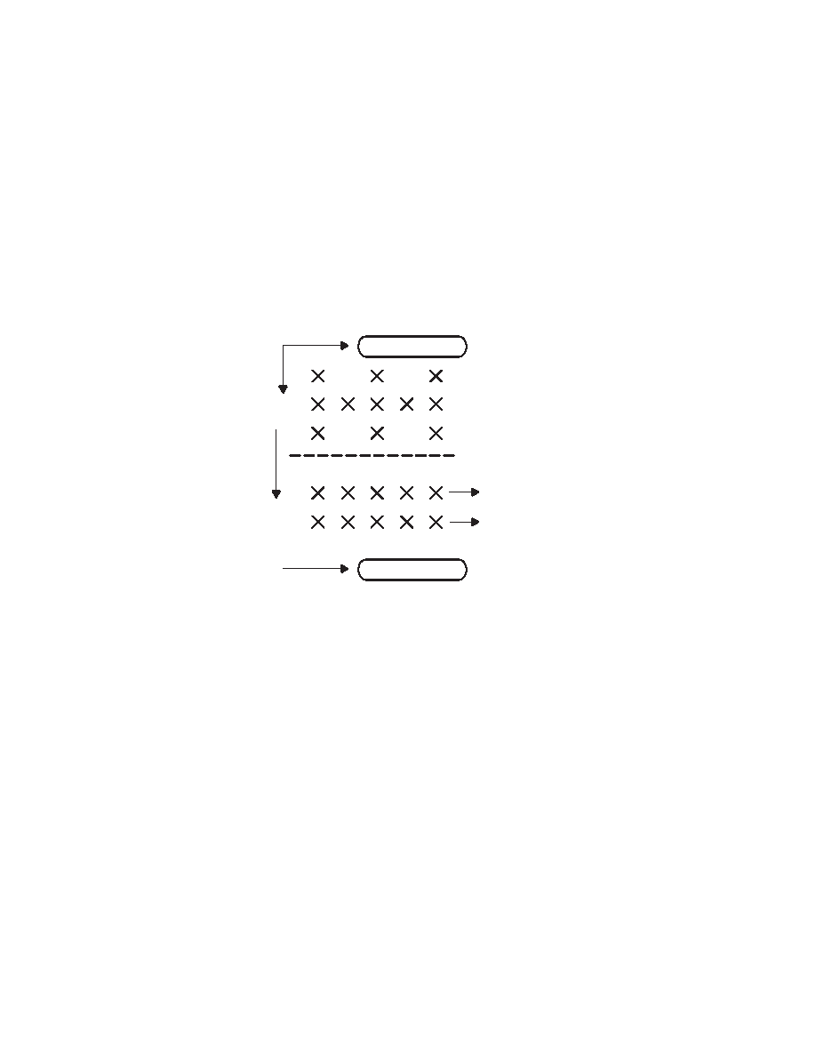
This block enables either a 4:4:4 24-bit output or 4:4:4 48-bit output at half the pixel clock or a 4:2:2 16-bit output,
useful for YUV digitizing (ITU.BT-601 style). In the latter case, an 8-bit port is used for the Y output, while a second
8-bit port is used alternately for Cr and Cb. As per ITU BT-601, Cb is the first video data word for each line, as shown
in Figure 2-7.
The first color sample after an incoming HS will be Cb. The output signal DHS is synchronized to the first pixel of a
line and can therefore be used to uniquely identify Cb from Cr output data in downsampled modes.
Cb
Cr
Cb
Cr
Cb
YY
Y
2 Channels
3 Channels
Cr (R-Y or V)
Cb (or B-Y or U)
Sampling Format
Y
X
Y
on Ch1 Bus A
Output
on Ch2 Bus A
Output
Other Outputs HI-Z
Output Format
t
Figure 2–7. Output Formatter
2.8
Power Down
In the I2C power-down register, four power down modes are defined:
Chip power down: PWDN_ALL
When PWDN_ALL=1, all analog circuits are powered down except the internal bandgap reference, the
circuit that generates the clamping voltages and the sync reference voltage. All these are kept active for
the composite sync slicer that remains active during power down. The clock frequency of the digital circuitry
will be lowered to reduce power consumption when in power down.
Internal reference power down: PWDN_REF
When PWDN_REF=1, bottom and top references (VREFB, VREFT) on all channels become inputs and
should be driven from external.
Bandgap reference power down: PWDN_BGAP
When PWDN_BGAP=1, the internal bandgap reference voltage is inactive and terminal VMID should be
driven from external.
DTO power down: DTO_DIS
When DTO_DIS=1, the DTO frequency is lowered to reduce power dissipation. When an external sampling
clock is used (EXT_ADCCLK), this power down can be activated.
相關PDF資料 |
PDF描述 |
|---|---|
| THS8083APZP | SPECIALTY CONSUMER CIRCUIT, PQFP100 |
| THS8083APZPG4 | SPECIALTY CONSUMER CIRCUIT, PQFP100 |
| THS8083CPZP | SPECIALTY CONSUMER CIRCUIT, PQFP100 |
| THS8133ACPHP | PARALLEL, WORD INPUT LOADING, 0.005 us SETTLING TIME, 10-BIT DAC, PQFP48 |
| THS8133BCPHP | PARALLEL, WORD INPUT LOADING, 0.005 us SETTLING TIME, 10-BIT DAC, PQFP48 |
相關代理商/技術參數 |
參數描述 |
|---|---|
| THS8083A | 制造商:TI 制造商全稱:Texas Instruments 功能描述:TRIPLE 8 BIT 80 MSPS 3.3V VIDEO AND GRAPHICS |
| THS8083A95 | 制造商:TI 制造商全稱:Texas Instruments 功能描述:TRIPLE 8-BIT, 95MSPS, 3.3V VIDEO AND GRAPHICS |
| THS8083A95PZP | 功能描述:視頻模擬/數字化轉換器集成電路 Tr 8B 95MSPS 3.3V Vid & Graphics Dig RoHS:否 制造商:Texas Instruments 輸入信號類型:Differential 轉換器數量:1 ADC 輸入端數量:4 轉換速率:3 Gbps 分辨率:8 bit 結構: 輸入電壓:3.3 V 接口類型:SPI 信噪比: 電壓參考: 電源電壓-最大:3.45 V 電源電壓-最小:3.15 V 最大功率耗散: 最大工作溫度:+ 85 C 最小工作溫度:- 40 C 封裝 / 箱體:TCSP-48 封裝:Reel |
| THS8083APZP | 功能描述:視頻模擬/數字化轉換器集成電路 Triple 8B 80 MSPS 3.3V YUV/RGB RoHS:否 制造商:Texas Instruments 輸入信號類型:Differential 轉換器數量:1 ADC 輸入端數量:4 轉換速率:3 Gbps 分辨率:8 bit 結構: 輸入電壓:3.3 V 接口類型:SPI 信噪比: 電壓參考: 電源電壓-最大:3.45 V 電源電壓-最小:3.15 V 最大功率耗散: 最大工作溫度:+ 85 C 最小工作溫度:- 40 C 封裝 / 箱體:TCSP-48 封裝:Reel |
| THS8083APZP | 制造商:Texas Instruments 功能描述:8BIT ADC 80MSPS TRIPLE SMD 8083 |
發布緊急采購,3分鐘左右您將得到回復。