- 您現在的位置:買賣IC網 > PDF目錄98229 > THS8083-95CPZP (TEXAS INSTRUMENTS INC) SPECIALTY CONSUMER CIRCUIT, PQFP100 PDF資料下載
參數資料
| 型號: | THS8083-95CPZP |
| 廠商: | TEXAS INSTRUMENTS INC |
| 元件分類: | 消費家電 |
| 英文描述: | SPECIALTY CONSUMER CIRCUIT, PQFP100 |
| 封裝: | POWER, THERMALLY ENHANCED, PLASTIC, TQFP-100 |
| 文件頁數: | 7/61頁 |
| 文件大小: | 239K |
| 代理商: | THS8083-95CPZP |
第1頁第2頁第3頁第4頁第5頁第6頁當前第7頁第8頁第9頁第10頁第11頁第12頁第13頁第14頁第15頁第16頁第17頁第18頁第19頁第20頁第21頁第22頁第23頁第24頁第25頁第26頁第27頁第28頁第29頁第30頁第31頁第32頁第33頁第34頁第35頁第36頁第37頁第38頁第39頁第40頁第41頁第42頁第43頁第44頁第45頁第46頁第47頁第48頁第49頁第50頁第51頁第52頁第53頁第54頁第55頁第56頁第57頁第58頁第59頁第60頁第61頁
2–1
2 Functional Description
2.1
Analog Channel
The THS8083 contains three identical analog channels that are independently programmable. Each channel consists
of a clamping circuit, a programmable gain amplifier, and an A/D converter.
2.2
Clamping Circuit
The purpose of clamping is to provide the input signal with a known dc-value. Typically, video signals will be
ac-coupled into the part. The signal needs to be level-shifted to fall in the reference voltage range (VREFB...VREFT)
of the A/D converter. By supplying a programmable clamp, the user can shift the input signal with respect to the A/D
range. This has the same effect as keeping the input signal constant and applying offset to both A/D reference
voltages while keeping the VREFT–VREFB difference equal. However, no external adjustments are needed with this
implementation.
For video, the clamping circuit can only be active during the non-active video portion of each line to avoid changes
in brightness along the line. Clamping is done during the horizontal blanking interval, either on the backporch of sync
or during the sync tip (in the case of a sync present on at least one of the video channels). If HS is carried on a separate
line, as is typically the case for PC graphics, clamping is done during blanking. When the Y or G input channel contains
an embedded sync, then alternatively clamping can be done during the sync-tip. This is not supported on the
THS8083, since it is expected that the input signal level during clamping (of which position and width are determined
by the clamp timing pulse, see later) corresponds to the blanking level. Since (for RGB type inputs) the blanking level
will correspond to a low output code of the A/D, it makes sense to center the clamp range around an A/D output code
of 0. The user can adjust this level up or down, symmetrically around 0. If the clamping is set such that the blanking
level corresponds to a level below 0, the A/D output is clipped at code 0.
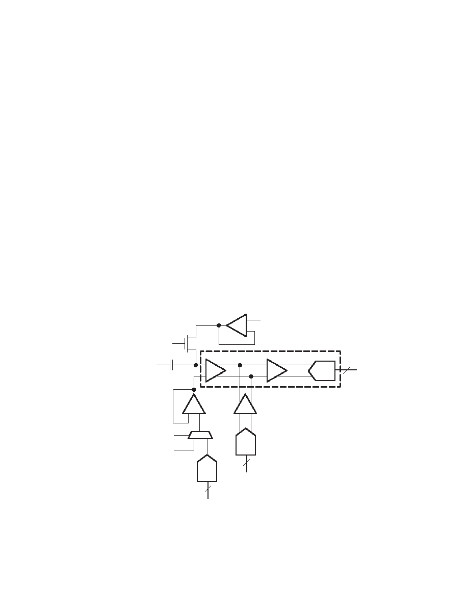
CLP
VIN
Reference Level
PGA 1
PGA 2
ADC
8
6
Reference Level
Bottom/Mid
8
Offset
DAC
Clamp DAC
PGA Gain Control
Clamp Control
CC
Figure 2–1. Analog Channel Architecture
In the case of YUV input signals, blanking levels for U and V correspond to the mid-level analog input. To handle these
signals the clamping range should be centered on the mid-level output code of the A/D.
相關PDF資料 |
PDF描述 |
|---|---|
| THS8083APZP | SPECIALTY CONSUMER CIRCUIT, PQFP100 |
| THS8083APZPG4 | SPECIALTY CONSUMER CIRCUIT, PQFP100 |
| THS8083CPZP | SPECIALTY CONSUMER CIRCUIT, PQFP100 |
| THS8133ACPHP | PARALLEL, WORD INPUT LOADING, 0.005 us SETTLING TIME, 10-BIT DAC, PQFP48 |
| THS8133BCPHP | PARALLEL, WORD INPUT LOADING, 0.005 us SETTLING TIME, 10-BIT DAC, PQFP48 |
相關代理商/技術參數 |
參數描述 |
|---|---|
| THS8083A | 制造商:TI 制造商全稱:Texas Instruments 功能描述:TRIPLE 8 BIT 80 MSPS 3.3V VIDEO AND GRAPHICS |
| THS8083A95 | 制造商:TI 制造商全稱:Texas Instruments 功能描述:TRIPLE 8-BIT, 95MSPS, 3.3V VIDEO AND GRAPHICS |
| THS8083A95PZP | 功能描述:視頻模擬/數字化轉換器集成電路 Tr 8B 95MSPS 3.3V Vid & Graphics Dig RoHS:否 制造商:Texas Instruments 輸入信號類型:Differential 轉換器數量:1 ADC 輸入端數量:4 轉換速率:3 Gbps 分辨率:8 bit 結構: 輸入電壓:3.3 V 接口類型:SPI 信噪比: 電壓參考: 電源電壓-最大:3.45 V 電源電壓-最小:3.15 V 最大功率耗散: 最大工作溫度:+ 85 C 最小工作溫度:- 40 C 封裝 / 箱體:TCSP-48 封裝:Reel |
| THS8083APZP | 功能描述:視頻模擬/數字化轉換器集成電路 Triple 8B 80 MSPS 3.3V YUV/RGB RoHS:否 制造商:Texas Instruments 輸入信號類型:Differential 轉換器數量:1 ADC 輸入端數量:4 轉換速率:3 Gbps 分辨率:8 bit 結構: 輸入電壓:3.3 V 接口類型:SPI 信噪比: 電壓參考: 電源電壓-最大:3.45 V 電源電壓-最小:3.15 V 最大功率耗散: 最大工作溫度:+ 85 C 最小工作溫度:- 40 C 封裝 / 箱體:TCSP-48 封裝:Reel |
| THS8083APZP | 制造商:Texas Instruments 功能描述:8BIT ADC 80MSPS TRIPLE SMD 8083 |
發布緊急采購,3分鐘左右您將得到回復。