- 您現在的位置:買賣IC網 > PDF目錄98282 > TPS53851RHHT (TEXAS INSTRUMENTS INC) SWITCHING CONTROLLER, PQCC36 PDF資料下載
參數資料
| 型號: | TPS53851RHHT |
| 廠商: | TEXAS INSTRUMENTS INC |
| 元件分類: | 穩壓器 |
| 英文描述: | SWITCHING CONTROLLER, PQCC36 |
| 封裝: | PLASTIC, VQFN-36 |
| 文件頁數: | 5/66頁 |
| 文件大小: | 1264K |
| 代理商: | TPS53851RHHT |
第1頁第2頁第3頁第4頁當前第5頁第6頁第7頁第8頁第9頁第10頁第11頁第12頁第13頁第14頁第15頁第16頁第17頁第18頁第19頁第20頁第21頁第22頁第23頁第24頁第25頁第26頁第27頁第28頁第29頁第30頁第31頁第32頁第33頁第34頁第35頁第36頁第37頁第38頁第39頁第40頁第41頁第42頁第43頁第44頁第45頁第46頁第47頁第48頁第49頁第50頁第51頁第52頁第53頁第54頁第55頁第56頁第57頁第58頁第59頁第60頁第61頁第62頁第63頁第64頁第65頁第66頁
www.ti.com
SLUS985 – DECEMBER 2009
4.3
VOLTAGE MASTER AND VOLTAGE SLAVE
A Voltage master has the channel that monitors the output voltage and generates the 'COMP' signal for
voltage regulation. A Voltage slave channel is configured by connecting the TRKx pin to BP5. Then the
COMP signal from the master is connected to the COMPx pin on the Voltage slave. When the TRKx pin is
connected to BP5 the COMPx output for that channel is put in a high impedance state, allowing the
regulation for that channel to be controlled by the Voltage master COMP signal.
4.3.1
TERMINAL FUNCTIONS
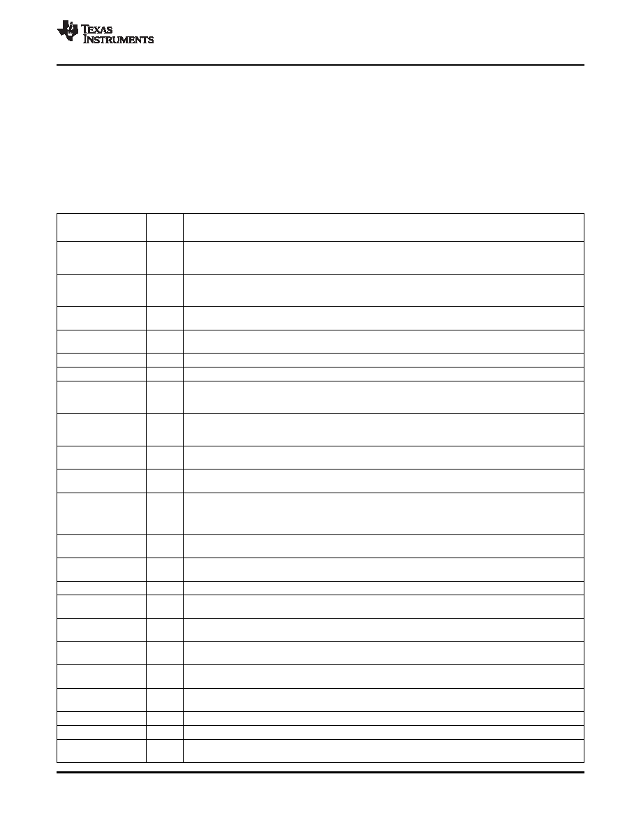
Table 4-1. TERMINAL FUNCTIONS
TERMINAL
I/O
DESCRIPTION
NAME
NO.
BOOT1 provides a bootstrapped supply for the high side FET driver for PWM1, enabling the gate of the
BOOT1
27
I
high side FET to be driven above the input supply rail. Connect a capacitor from BOOT1 to SW1 pin and
a Schottky diode from this pin to VREG.
BOOT2 provides a bootstrapped supply for the high side FET driver for PWM2, enabling the gate of the
BOOT2
18
I
high side FET to be driven above the input supply rail. Connect a capacitor from BOOT2 to SW2 pin and
a Schottky diode from this pin to VREG.
Filtered input from the VREG pin. A 10-
resistor should be connected between VREG and BP5 and a
BP5
8
I
1.0-
μF ceramic capacitor should be connected from BP5 to ground.
Digital clock signal for synchronizing slave controllers to the master CLKIO frequency and is either 6 or 8
CLKIO
28
O
times the PWM switching frequency.
COMP1
35
O
Output of the error amplifier, CH1. The voltage at this pin determines the duty cycle for the PWM1.
COMP2
10
O
Output of the error amplifier, CH2. The voltage at this pin determines the duty cycle for the PWM2.
These pins are used to sense the CH1 phase current. Inductor current can be sensed with an external
CS1
31
I
current sense resistor or by using an external R-C circuit and the inductor’s DC resistance. The traces for
these signals must be connected directly at the current sense element.
These pins are used to sense the CH2 phase current. Inductor current can be sensed with an external
CS2
14
I
current sense resistor or by using an external R-C circuit and the inductor’s DC resistance. The traces for
these signals must be connected directly at the current sense element.
Return point of CH1 current sense voltage. The trace for this signal must be connected directly at the
CSRT1
32
I
current sense element.
Return point of CH1 current sense voltage. The trace for this signal must be connected directly at the
CSRT2
13
I
current sense element.
Output of the differential amplifier. The output voltage of the differential amplifier is limited to 5.8 V. For
remote sensing, the voltage at this pin represents the true output voltage without I × R drops that result
DIFFO
1
O
from high current in the PCB traces. The VOUT and GSNS pins must be connected directly at the point of
load where regulation is required. See Layout Guidelines for more information.
Inverting input of the error amplifier for CH1. In closed loop operation, the voltage at this pin is nominally
FB1
36
I
700 mV. This pin is also monitored for PGOOD1 and undervoltage on CH1.
Inverting input of the error amplifier for CH2. In closed loop operation, the voltage at this pin is nominally
FB2
9
I
700 mV. This pin is also monitored for PGOOD2 and undervoltage on CH2.
GND
7
-
Low noise ground connection to the device.
Inverting input of the differential amplifier. This pin should be connected to ground at the load. If the
GSNS
3
I
differential amplifier is not used, tie this pin to GND or leave open.
Gate drive output for the high side N-channel MOSFET switch for CH1. Output is referenced to SW1 and
HDRV1
26
O
is bootstrapped for enhancement of the high side switch.
Gate drive output for the high side N-channel MOSFET switch for CH2. Output is referenced to SW2 and
HRDV2
19
O
is bootstrapped for enhancement of the high side switch.
Used to set the cycle-by-cycle current limit threshold for CH1. If the ILIM1 threshold is reached, the PWM
ILIM1
34
I
pulse is terminated and the converter delivers limited current to the output.
Used to set the cycle-by-cycle current limit threshold for CH2. If the ILIM2 threshold is reached, the PWM
ILIM2
11
I
pulse is terminated and the converter delivers limited current to the output.
LRDV1
24
O
Gate drive output for the low side synchronous rectifier (SR) N-channel MOSFET for CH1.
LRDV2
22
O
Gate drive output for the low side synchronous rectifier (SR) N-channel MOSFET for CH2.
Power ground reference for the controller lower gate drivers. There should be a high current return path
PGND
23
-
from the sources of the lower MOSFETs to this pin.
Copyright 2009, Texas Instruments Incorporated
DEVICE INFORMATION
13
Product Folder Link(s): TPS53851
相關PDF資料 |
PDF描述 |
|---|---|
| TPS54010PWPG4 | 25 A SWITCHING REGULATOR, 762 kHz SWITCHING FREQ-MAX, PDSO28 |
| TPS54040DGQ | 0.5 A SWITCHING REGULATOR, 2500 kHz SWITCHING FREQ-MAX, PDSO10 |
| TPS54073PWPRG4 | 25 A SWITCHING REGULATOR, 762 kHz SWITCHING FREQ-MAX, PDSO28 |
| TPS54073PWPR | 25 A SWITCHING REGULATOR, 762 kHz SWITCHING FREQ-MAX, PDSO28 |
| TPS54073PWP | 25 A SWITCHING REGULATOR, 762 kHz SWITCHING FREQ-MAX, PDSO28 |
相關代理商/技術參數 |
參數描述 |
|---|---|
| TPS53915EVM-587 | 功能描述:TPS53915 SWIFT?, D-CAP3?, Eco-Mode? DC/DC, Step Down 1, Non-Isolated Outputs Evaluation Board 制造商:texas instruments 系列:SWIFT?,D-CAP3?,Eco-Mode? 零件狀態:有效 主要用途:DC/DC,步降 輸出和類型:1,非隔離 功率 - 輸出:- 電壓 - 輸出:1.2V 電流 - 輸出:12A 電壓 - 輸入:12V 穩壓器拓撲:降壓 頻率 - 開關:- 板類型:完全填充 所含物品:板 使用的 IC/零件:TPS53915 標準包裝:1 |
| TPS53915RVET | 制造商:Texas Instruments 功能描述:1.5V TO 18V INPUT (4.5V TO 25V BIAS), 12-A SYNCHRONOUS STEP- - Tape and Reel 制造商:Texas Instruments 功能描述:IC REG BUCK SYNC ADJ 12A 28VQFN |
| TPS5401 | 制造商:TI 制造商全稱:Texas Instruments 功能描述:0.5-A, 42-V Input, Step-Down SWIFT? Converter |
| TPS54010 | 制造商:TI 制造商全稱:Texas Instruments 功能描述:SWIFT Converter Product Portfolio |
| TPS54010EVM-067 | 功能描述:電源管理IC開發工具 4.0 Vin DC/DC Conv RoHS:否 制造商:Maxim Integrated 產品:Evaluation Kits 類型:Battery Management 工具用于評估:MAX17710GB 輸入電壓: 輸出電壓:1.8 V |
發布緊急采購,3分鐘左右您將得到回復。