- 您現在的位置:買賣IC網 > PDF目錄98287 > TS8387VF_ 1-CH 8-BIT PROPRIETARY METHOD ADC, PARALLEL ACCESS, CQFP68 PDF資料下載
參數資料
| 型號: | TS8387VF_ |
| 元件分類: | ADC |
| 英文描述: | 1-CH 8-BIT PROPRIETARY METHOD ADC, PARALLEL ACCESS, CQFP68 |
| 封裝: | CERAMIC, QFP-68 |
| 文件頁數: | 19/38頁 |
| 文件大小: | 617K |
| 代理商: | TS8387VF_ |
第1頁第2頁第3頁第4頁第5頁第6頁第7頁第8頁第9頁第10頁第11頁第12頁第13頁第14頁第15頁第16頁第17頁第18頁當前第19頁第20頁第21頁第22頁第23頁第24頁第25頁第26頁第27頁第28頁第29頁第30頁第31頁第32頁第33頁第34頁第35頁第36頁第37頁第38頁
TS8387
26/38
Example given : Using the 10E452 register:
Minimum Setup time : 150 ps
Minimum Hold time : 200 ps
As a consequence, it is recommended to use the Data Ready ( DR,DRB) signal for storing the output datas by external
latches or by the digital acquisition system, as ( DR,DRB ) tracks the data output propagation delay ( TOD ) in the whole
temperature range.
7.2.
ANALOG INPUTS (VIN) (VINB)
The analog input Full Scale range is 0.5 Volts peak to peak (Vpp).
In differential mode input configuration, that means 0.25 Volt on each input, or +/– 125 mV around zero volt. The input
common mode is GROUND.
The typical input capacitance is 3 pF for TS8387 in CQFP package.
The input capacitance is mainly due to the package.(note : the ESD protections are not connected(but present) on the
inputs.
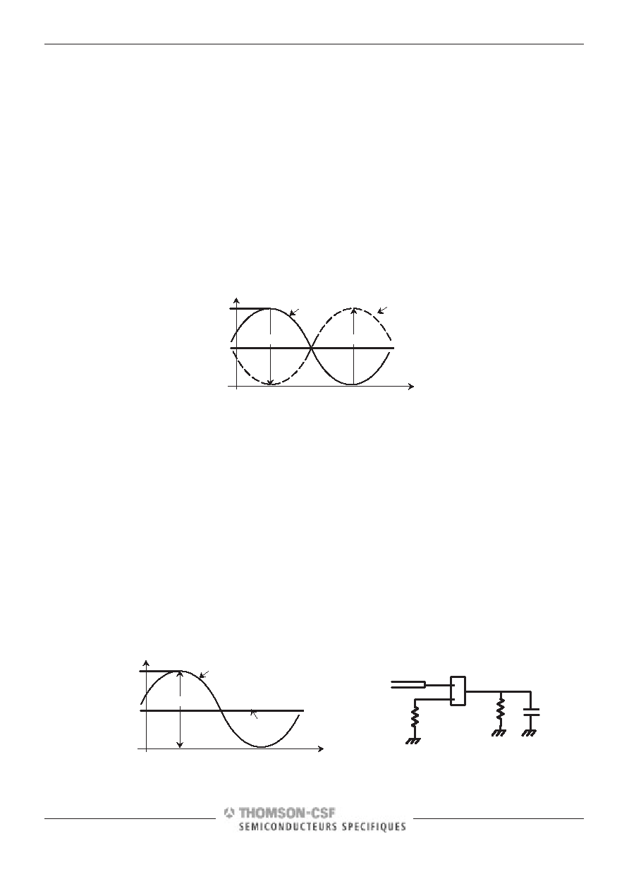
Differential inputs voltage span
–125
125
[mV]
–250 mV
250 mV
VIN
500mV
Full Scale
analog input
t
VINB
(VIN,VINB)=+/– 250 mV = 500 mV diff
0 Volt
Differential versus single ended analog input operation
The TS8387 can operate at full speed without any performance degradation in either differential or single ended config-
uration.
This is explained by the fact the ADC uses a high input impedance differential preamplifier stage, (preceding the master/
slave Track and Hold stage), which has been designed in order to be entered either in differential mode or single-ended
mode.
This is true so long as the out of phase analog input pad VINB is 50 ohms terminated very closely to one of the neighbor-
ing ground pins (52,53,58,59) which constitute the local ground reference for the inphase analog input pad (VIN).
Thus the differential analog input preamplifier will fully reject the local ground noise ( and any capacitively and induc-
tively coupled noise) as common mode effects.
In typical single-ended configuration, enter on the (VIN) input pad, with the inverted phase input pad (VINB) grounded
through the 50 ohms termination resistor.
In single-ended input configuration, the in–phase input amplitude is 0.5 Volt peak to peak,centered on 0V. (or –2 dBm
into 50 ohms.)
The inverted phase input is at ground potential through the 50 ohms termination resistor.
Typical Single ended analog input configuration
–250
250
[mV]
500 mV
Full Scale
analog input
t
VIN = ±250 mV 500 mVpp diff
VINB
VIN
VINB = 0V
VIN or VINB
VIN or VINB double pad
50
(external)
50
reverse termination
1M
0.4 pF
相關PDF資料 |
PDF描述 |
|---|---|
| TS12A4516P | 1-CHANNEL, SGL POLE SGL THROW SWITCH, PDIP8 |
| TS2007EIJT | 3 W, 1 CHANNEL, AUDIO AMPLIFIER, PBGA9 |
| TS2007EKIJT | 3 W, 1 CHANNEL, AUDIO AMPLIFIER, PBGA9 |
| TS2007IQT | 2.3 W, 1 CHANNEL, AUDIO AMPLIFIER, DSO8 |
| TS2012EIJT | 2.5 W, 2 CHANNEL, AUDIO AMPLIFIER, PBGA16 |
相關代理商/技術參數 |
參數描述 |
|---|---|
| TS8388B | 制造商:ATMEL 制造商全稱:ATMEL Corporation 功能描述:ADC 8-bit 1 GSPS |
| TS8388BCF | 制造商:e2v technologies 功能描述:ADC 8-BIT 1 GSPS - Trays |
| TS8388BCFS | 制造商:e2v technologies 功能描述:ADC 8-BIT 1 GSPS - Trays |
| TS8388BCG | 制造商:未知廠家 制造商全稱:未知廠家 功能描述:A/D CONVERTER |
| TS8388BCGL | 制造商:e2v technologies 功能描述:ADC 8-BIT 1 GSPS - Trays |
發布緊急采購,3分鐘左右您將得到回復。