- 您現在的位置:買賣IC網 > PDF目錄365986 > TSPC106AMGS83CE MEMORY CONTROLLER PDF資料下載
參數資料
| 型號: | TSPC106AMGS83CE |
| 英文描述: | MEMORY CONTROLLER |
| 中文描述: | 內存控制器 |
| 文件頁數: | 12/40頁 |
| 文件大小: | 569K |
| 代理商: | TSPC106AMGS83CE |
第1頁第2頁第3頁第4頁第5頁第6頁第7頁第8頁第9頁第10頁第11頁當前第12頁第13頁第14頁第15頁第16頁第17頁第18頁第19頁第20頁第21頁第22頁第23頁第24頁第25頁第26頁第27頁第28頁第29頁第30頁第31頁第32頁第33頁第34頁第35頁第36頁第37頁第38頁第39頁第40頁
12
TSPC106
2102B
–
HIREL
–
02/02
L2 Cache/Multiple
Processor Interface
Signals
The TSPC106 provides support for either an internal L2 cache controller or an external
L2 cache controller and/or additional 60x processors.
Internal L2 Controller Signals
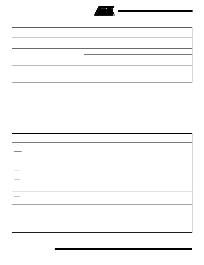
Table 3 lists the interface signals for the internal L2 controller and provides a brief
description of their functions. The internal L2 controller supports either burst SRAMs or
asynchronous SRAMs. Some of the signals perform different functions depending on
the SRAM configuration.
TSIZ[0:2]
Transfer size
3
O
Specifies the data transfer size for the 60x bus transaction.
I
Specifies the data transfer size for the 60x bus transaction.
TT[0:4]
Transfer type
5
O
Specifies the type of 60x bus transfer in progress.
I
Specifies the type of 60x bus transfer in progress.
WT
Write-through
1
I/O
Indicates that an access is write-through.
XATS
Extended address
transfer start
1
I
Indicates that the 60x has started a direct-store access (using the
extended transfer protocol). Since direct-store accesses are not
supported by the TSPC106, the TSPC106 automatically asserts when
TEA and XATS are asserted (provided TEA is enabled).
Table 2.
60x Processor Interface Signals (Continued)
Signal
Signal Name
Number of
Pins
I/O
Signal Description
Table 3.
Internal L2 Controller Signals
Signal
Signal Name
Number of
Pins
I/O
Signal Description
ADS
DALE
BRL2
Address strobe
1
O
For a burst SRAM configuration, indicates to the burst SRAM that the
address is valid to be latched.
BA0
BR3
Burst address 0
1
I/O
For an asynchronous SRAM configuration, indicates bit 0 of the burst
address counter.
BA1
BAA
BGL2
Burst address 1
1
O
For an asynchronous SRAM configuration, indicates bit 1 of the burst
address counter.
BAA
BA1
BGL2
Bus address
advance
1
O
For a burst SRAM configuration, indicates that the burst RAMs should
increment their internal addresses.
DALE
ADS
BRL2
Data address latch
enable
1
O
For an asynchronous SRAM configuration, indicates that the external
address latch should latch the current 60x bus address.
DCS
BG3
Data RAM chip
select
1
O
Enables the L2 data RAMs for a read or write operation.
DIRTY_IN
BR1
Dirty in
1
I
Indicates that the selected L2 cache line is modified. The polarity of
DIRTY_IN is programmable.
DIRTY_OUT
BG1
Dirty out
1
O
Indicates that the L2 cache line should be marked as modified. The
polarity of DIRTY_OUT is programmable.
相關PDF資料 |
PDF描述 |
|---|---|
| TSPC106AMGS83CG | MEMORY CONTROLLER |
| TSPC106AVGU66CE | MEMORY CONTROLLER |
| TSPC106AVGU66CG | MEMORY CONTROLLER |
| TSPC106AVGU83CE | MEMORY CONTROLLER |
| TSPC106AVGU83CG | MEMORY CONTROLLER |
相關代理商/技術參數 |
參數描述 |
|---|---|
| TSPC106AMGS83CG | 制造商:未知廠家 制造商全稱:未知廠家 功能描述:MEMORY CONTROLLER |
| TSPC106AMGSB/Q66CE | 制造商:未知廠家 制造商全稱:未知廠家 功能描述:MEMORY CONTROLLER |
| TSPC106AMGSB/Q66CG | 制造商:未知廠家 制造商全稱:未知廠家 功能描述:MEMORY CONTROLLER |
| TSPC106AMGSB/Q83CE | 制造商:未知廠家 制造商全稱:未知廠家 功能描述:MEMORY CONTROLLER |
| TSPC106AMGSB/Q83CG | 制造商:未知廠家 制造商全稱:未知廠家 功能描述:MEMORY CONTROLLER |
發布緊急采購,3分鐘左右您將得到回復。