- 您現在的位置:買賣IC網 > PDF目錄365986 > TSPC106AMGS83CE MEMORY CONTROLLER PDF資料下載
參數資料
| 型號: | TSPC106AMGS83CE |
| 英文描述: | MEMORY CONTROLLER |
| 中文描述: | 內存控制器 |
| 文件頁數: | 18/40頁 |
| 文件大小: | 569K |
| 代理商: | TSPC106AMGS83CE |
第1頁第2頁第3頁第4頁第5頁第6頁第7頁第8頁第9頁第10頁第11頁第12頁第13頁第14頁第15頁第16頁第17頁當前第18頁第19頁第20頁第21頁第22頁第23頁第24頁第25頁第26頁第27頁第28頁第29頁第30頁第31頁第32頁第33頁第34頁第35頁第36頁第37頁第38頁第39頁第40頁
18
TSPC106
2102B
–
HIREL
–
02/02
Interrupt, Clock and Power Management Signals
The TSPC106 coordinates interrupt, clocking, and power management signals across the memory bus, the PCI bus and
the 60x processor bus.
IEEE 1149.1 Interface Signals
To facilitate system testing, the TSPC106 provides a JTAG test access port that complies with the IEEE 1149.1 boundary-
scan specification.
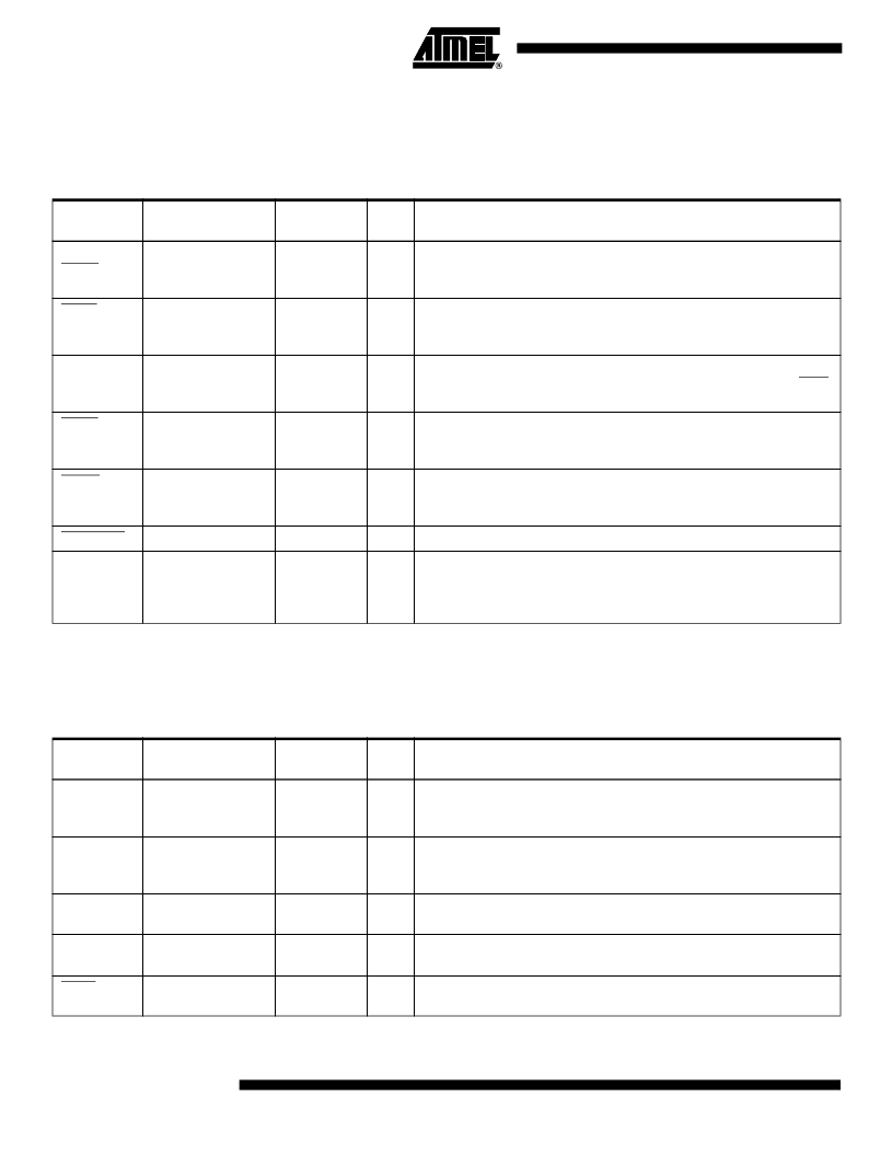
Table 8.
Interrupt, Clock and Power Management Signals
Signal
Signal Name
Number of
Pins
I/O
Signal Description
CKO
DWE2
Test clock
1
O
CKO provides a means to monitor the internal PLL output or the bus
clock frequency. The CKO clock should be used for testing purposes
only. It is not intended as a reference clock signal.
HRST
Hard reset
1
I
Initiates a complete hard reset of the TSPC106. During assertion, all
bi-directional signals are released to a high-impedance state and all
output signals are either in a high impedance or inactive state.
NMI
Nonmaskable
interrupt
1
I
Indicates that an external device (typically an interrupt controller) has
detected a catastrophic error. In response, the TSPC106 asserts MCP
on the 60x processor bus.
QACK
Quiesce
acknowledge
1
O
Indicates that the TSPC106 is in a low-power state. All bus activity that
requires snooping has terminated and the 60x processor may enter a
low-power state.
QREQ
Quiesce request
1
I
Indicates that a 60x processor is requesting that all bus activity
involving snoop operations pause or terminate so that the 60x
processor may enter a low-power state.
SUSPEND
Suspend
1
I
Activates the suspend power-saving mode.
SYSCLK
System clock
1
I
SYSCLK sets the frequency of operation for the PCI bus and provides
a reference clock for the phase-locked loop (PLL) in the TSPC106.
SYSCLK is used to synchronize bus operations. Refer to section
“
Clocking
”
on page 19 for more information.
Table 9.
IEEE 1149.1 Interface Signals
Signal
Signal Name
Number of
Pins
I/O
Signal Description
TCK
JTAG test clock
1
I
Input signals to the test access port (TAP) are clocked in on the rising
edge of TCK. Changes to the TAP output signals occur on the falling
edge of TCK. The test logic allows TCK to be stopped.
TDO
JTAG test data
output
1
O
The contents of the selected internal instructions or data register are
shifted out onto this signal on the falling edge of TCK. TDO will remain
in a high-impedance state except when scanning of data is in progress.
TDI
JTAG test data
input
1
I
The value presented on this signal on the rising edge of TCK is clocked
into the selected JTAG test instruction or data register.
TMS
JTAG test mode
select
1
I
This signal is decoded by the internal JTAG TAP controller to
distinguish the primary operation of the test support circuitry.
TRST
JTAG test reset
1
I
This input causes asynchronous initialization of the internal JTAG TAP
controller.
相關PDF資料 |
PDF描述 |
|---|---|
| TSPC106AMGS83CG | MEMORY CONTROLLER |
| TSPC106AVGU66CE | MEMORY CONTROLLER |
| TSPC106AVGU66CG | MEMORY CONTROLLER |
| TSPC106AVGU83CE | MEMORY CONTROLLER |
| TSPC106AVGU83CG | MEMORY CONTROLLER |
相關代理商/技術參數 |
參數描述 |
|---|---|
| TSPC106AMGS83CG | 制造商:未知廠家 制造商全稱:未知廠家 功能描述:MEMORY CONTROLLER |
| TSPC106AMGSB/Q66CE | 制造商:未知廠家 制造商全稱:未知廠家 功能描述:MEMORY CONTROLLER |
| TSPC106AMGSB/Q66CG | 制造商:未知廠家 制造商全稱:未知廠家 功能描述:MEMORY CONTROLLER |
| TSPC106AMGSB/Q83CE | 制造商:未知廠家 制造商全稱:未知廠家 功能描述:MEMORY CONTROLLER |
| TSPC106AMGSB/Q83CG | 制造商:未知廠家 制造商全稱:未知廠家 功能描述:MEMORY CONTROLLER |
發布緊急采購,3分鐘左右您將得到回復。