- 您現在的位置:買賣IC網 > PDF目錄21981 > XC3S1600E-4FGG400C (Xilinx Inc)IC SPARTAN-3E FPGA 1600K 400FBGA PDF資料下載
參數資料
| 型號: | XC3S1600E-4FGG400C |
| 廠商: | Xilinx Inc |
| 文件頁數: | 161/227頁 |
| 文件大小: | 0K |
| 描述: | IC SPARTAN-3E FPGA 1600K 400FBGA |
| 產品培訓模塊: | FPGAs Spartan3 |
| 標準包裝: | 60 |
| 系列: | Spartan®-3E |
| LAB/CLB數: | 3688 |
| 邏輯元件/單元數: | 33192 |
| RAM 位總計: | 663552 |
| 輸入/輸出數: | 304 |
| 門數: | 1600000 |
| 電源電壓: | 1.14 V ~ 1.26 V |
| 安裝類型: | 表面貼裝 |
| 工作溫度: | 0°C ~ 85°C |
| 封裝/外殼: | 400-BGA |
| 供應商設備封裝: | 400-FBGA(21x21) |
| 配用: | HW-XA3S1600E-UNI-G-ND - KIT DEVELOPMENT AUTOMOTIVE ECU |
| 其它名稱: | 122-1517 |
第1頁第2頁第3頁第4頁第5頁第6頁第7頁第8頁第9頁第10頁第11頁第12頁第13頁第14頁第15頁第16頁第17頁第18頁第19頁第20頁第21頁第22頁第23頁第24頁第25頁第26頁第27頁第28頁第29頁第30頁第31頁第32頁第33頁第34頁第35頁第36頁第37頁第38頁第39頁第40頁第41頁第42頁第43頁第44頁第45頁第46頁第47頁第48頁第49頁第50頁第51頁第52頁第53頁第54頁第55頁第56頁第57頁第58頁第59頁第60頁第61頁第62頁第63頁第64頁第65頁第66頁第67頁第68頁第69頁第70頁第71頁第72頁第73頁第74頁第75頁第76頁第77頁第78頁第79頁第80頁第81頁第82頁第83頁第84頁第85頁第86頁第87頁第88頁第89頁第90頁第91頁第92頁第93頁第94頁第95頁第96頁第97頁第98頁第99頁第100頁第101頁第102頁第103頁第104頁第105頁第106頁第107頁第108頁第109頁第110頁第111頁第112頁第113頁第114頁第115頁第116頁第117頁第118頁第119頁第120頁第121頁第122頁第123頁第124頁第125頁第126頁第127頁第128頁第129頁第130頁第131頁第132頁第133頁第134頁第135頁第136頁第137頁第138頁第139頁第140頁第141頁第142頁第143頁第144頁第145頁第146頁第147頁第148頁第149頁第150頁第151頁第152頁第153頁第154頁第155頁第156頁第157頁第158頁第159頁第160頁當前第161頁第162頁第163頁第164頁第165頁第166頁第167頁第168頁第169頁第170頁第171頁第172頁第173頁第174頁第175頁第176頁第177頁第178頁第179頁第180頁第181頁第182頁第183頁第184頁第185頁第186頁第187頁第188頁第189頁第190頁第191頁第192頁第193頁第194頁第195頁第196頁第197頁第198頁第199頁第200頁第201頁第202頁第203頁第204頁第205頁第206頁第207頁第208頁第209頁第210頁第211頁第212頁第213頁第214頁第215頁第216頁第217頁第218頁第219頁第220頁第221頁第222頁第223頁第224頁第225頁第226頁第227頁
Spartan-3E FPGA Family: Functional Description
DS312 (v4.1) July 19, 2013
Product Specification
39
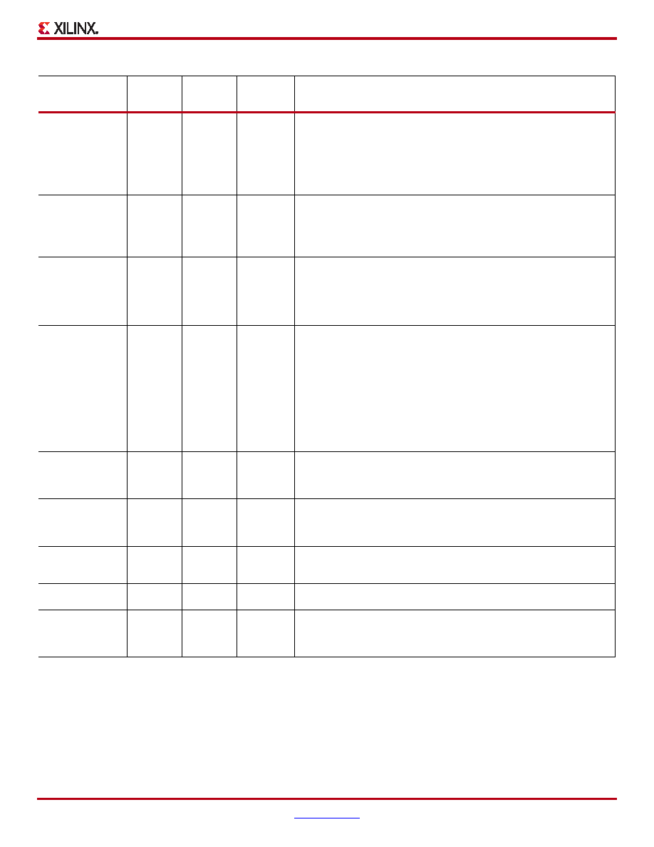
Table 23: Block RAM Port Signals
Signal
Description
Port A
Signal
Name
Port B
Signal
Name
Direction
Function
Address Bus
ADDRA
ADDRB
Input
The Address Bus selects a memory location for read or write operations.
The width (w) of the port’s associated data path determines the number of
available address lines (r), as per Table 22.
Whenever a port is enabled (ENA or ENB = High), address transitions must
meet the data sheet setup and hold times with respect to the port clock
(CLKA or CLKB), as shown in Table 103, page 139.This requirement must
be met even if the RAM read output is of no interest.
Data Input Bus
DIA
DIB
Input
Data at the DI input bus is written to the RAM location specified by the
address input bus (ADDR) during the active edge of the CLK input, when
the clock enable (EN) and write enable (WE) inputs are active.
It is possible to configure a port’s DI input bus width (w-p) based on
Table 22. This selection applies to both the DI and DO paths of a given port.
Parity Data Input(s)
DIPA
DIPB
Input
Parity inputs represent additional bits included in the data input path.
Although referred to herein as “parity” bits, the parity inputs and outputs
have no special functionality for generating or checking parity and can be
used as additional data bits. The number of parity bits ‘p’ included in the DI
(same as for the DO bus) depends on a port’s total data path width (w). See
Data Output Bus
DOA
DOB
Output
Data is written to the DO output bus from the RAM location specified by the
address input bus, ADDR. See the DI signal description for DO port width
configurations.
Basic data access occurs on the active edge of the CLK when WE is
inactive and EN is active. The DO outputs mirror the data stored in the
address ADDR memory location. Data access with WE active if the
WRITE_MODE attribute is set to the value: WRITE_FIRST, which
accesses data after the write takes place. READ_FIRST accesses data
before the write occurs. A third attribute, NO_CHANGE, latches the DO
outputs upon the assertion of WE. See Block RAM Data Operations for
details on the WRITE_MODE attribute.
Parity Data
Output(s)
DOPA
DOPB
Output
Parity outputs represent additional bits included in the data input path. The
number of parity bits ‘p’ included in the DI bus (same as for the DO bus)
depends on a port’s total data path width (w). See the DIP signal
description for configuration details.
Write Enable
WEA
WEB
Input
When asserted together with EN, this input enables the writing of data to
the RAM. When WE is inactive with EN asserted, read operations are still
possible. In this case, a latch passes data from the addressed memory
location to the DO outputs.
Clock Enable
ENA
ENB
Input
When asserted, this input enables the CLK signal to perform read and write
operations to the block RAM. When inactive, the block RAM does not
perform any read or write operations.
Set/Reset
SSRA
SSRB
Input
When asserted, this pin forces the DO output latch to the value of the
SRVAL attribute. It is synchronized to the CLK signal.
Clock
CLKA
CLKB
Input
This input accepts the clock signal to which read and write operations are
synchronized. All associated port inputs are required to meet setup times
with respect to the clock signal’s active edge. The data output bus responds
after a clock-to-out delay referenced to the clock signal’s active edge.
相關PDF資料 |
PDF描述 |
|---|---|
| TPSD227K004R0100 | CAP TANT 220UF 4V 10% 2917 |
| HCC43DRAN-S734 | CONN EDGECARD 86POS .100 R/A PCB |
| VJ1206Y181KBAAT4X | CAP CER 180PF 50V 10% X7R 1206 |
| HCC43DRAH-S734 | CONN EDGECARD 86POS .100 R/A PCB |
| RW2-2415S/H3/SMD | CONV DC/DC 2W 18-36VIN 15VOUT |
相關代理商/技術參數 |
參數描述 |
|---|---|
| XC3S1600E-4FGG400I | 功能描述:IC FPGA SPARTAN-3E 1600K 400FBGA RoHS:是 類別:集成電路 (IC) >> 嵌入式 - FPGA(現場可編程門陣列) 系列:Spartan®-3E 標準包裝:40 系列:Spartan® 6 LX LAB/CLB數:3411 邏輯元件/單元數:43661 RAM 位總計:2138112 輸入/輸出數:358 門數:- 電源電壓:1.14 V ~ 1.26 V 安裝類型:表面貼裝 工作溫度:-40°C ~ 100°C 封裝/外殼:676-BGA 供應商設備封裝:676-FBGA(27x27) |
| XC3S1600E-4FGG484C | 制造商:Xilinx 功能描述:FPGA SPARTAN-3E 1.6M GATES 33192 CELLS 572MHZ 90NM 1.2V 484F - Trays 制造商:Xilinx 功能描述:FPGA SPARTAN-3E 1600K GATES 484FBGA |
| XC3S1600E-4FGG484I | 功能描述:IC FPGA SPARTAN-3E 1600K 484FBGA RoHS:是 類別:集成電路 (IC) >> 嵌入式 - FPGA(現場可編程門陣列) 系列:Spartan®-3E 產品變化通告:Step Intro and Pkg Change 11/March/2008 標準包裝:1 系列:Virtex®-5 SXT LAB/CLB數:4080 邏輯元件/單元數:52224 RAM 位總計:4866048 輸入/輸出數:480 門數:- 電源電壓:0.95 V ~ 1.05 V 安裝類型:表面貼裝 工作溫度:-40°C ~ 100°C 封裝/外殼:1136-BBGA,FCBGA 供應商設備封裝:1136-FCBGA 配用:568-5088-ND - BOARD DEMO DAC1408D750122-1796-ND - EVALUATION PLATFORM VIRTEX-5 |
| XC3S1600E-4FT256C | 制造商:XILINX 制造商全稱:XILINX 功能描述:Spartan-3E FPGA Family |
| XC3S1600E-4FT256I | 制造商:XILINX 制造商全稱:XILINX 功能描述:Spartan-3E FPGA Family |
發布緊急采購,3分鐘左右您將得到回復。