- 您現在的位置:買賣IC網 > PDF目錄36340 > 935269343557 (NXP SEMICONDUCTORS) SPECIALTY CONSUMER CIRCUIT, PQFP160 PDF資料下載
參數資料
| 型號: | 935269343557 |
| 廠商: | NXP SEMICONDUCTORS |
| 元件分類: | 消費家電 |
| 英文描述: | SPECIALTY CONSUMER CIRCUIT, PQFP160 |
| 封裝: | 28 X 28 MM, 3.40 MM HEIGHT, ROHS COMPLIANT, PLASTIC, SOT322-2, MS-022, QFP-160 |
| 文件頁數: | 114/143頁 |
| 文件大?。?/td> | 696K |
| 代理商: | 935269343557 |
第1頁第2頁第3頁第4頁第5頁第6頁第7頁第8頁第9頁第10頁第11頁第12頁第13頁第14頁第15頁第16頁第17頁第18頁第19頁第20頁第21頁第22頁第23頁第24頁第25頁第26頁第27頁第28頁第29頁第30頁第31頁第32頁第33頁第34頁第35頁第36頁第37頁第38頁第39頁第40頁第41頁第42頁第43頁第44頁第45頁第46頁第47頁第48頁第49頁第50頁第51頁第52頁第53頁第54頁第55頁第56頁第57頁第58頁第59頁第60頁第61頁第62頁第63頁第64頁第65頁第66頁第67頁第68頁第69頁第70頁第71頁第72頁第73頁第74頁第75頁第76頁第77頁第78頁第79頁第80頁第81頁第82頁第83頁第84頁第85頁第86頁第87頁第88頁第89頁第90頁第91頁第92頁第93頁第94頁第95頁第96頁第97頁第98頁第99頁第100頁第101頁第102頁第103頁第104頁第105頁第106頁第107頁第108頁第109頁第110頁第111頁第112頁第113頁當前第114頁第115頁第116頁第117頁第118頁第119頁第120頁第121頁第122頁第123頁第124頁第125頁第126頁第127頁第128頁第129頁第130頁第131頁第132頁第133頁第134頁第135頁第136頁第137頁第138頁第139頁第140頁第141頁第142頁第143頁
2004 Aug 25
72
Philips Semiconductors
Product specication
Multimedia bridge, high performance
Scaler and PCI circuit (SPCI)
SAA7146A
The PCI source data is defined by the base address
(BaseOdd3 and BaseEven3), the distance between the
start addresses of two consecutive lines of a field (Pitch3),
the number of lines per field of the source frame
(NumLines3) and the number of bytes per line of the
source frame (NumByte3). The programmer must provide
correct scaling settings to fulfil the target window
requirements. The pitch has to be Dword aligned.
7.10.2
PLAYBACK MODE
The SAA7146A offers three different modes to support the
playback mode for various systems. The Binary Ratio
Scaler (BRS) inputs data from FIFO 3, therefore the DMA3
is in master read operation. The scaling result is passed to
the DD1 output.
The following sections describe the three different modes:
field memory mode, direct mode and line memory mode.
7.10.2.1
Field memory mode
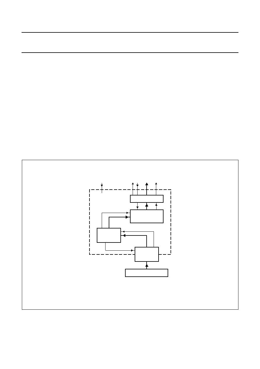
In the field memory mode the SAA7146A takes a vertical
sync signal as a timing reference signal. A reset signal for
a field memory and a PXQ as write enable are generated
within the circuit and both are sent to port A or port B.
In this mode the pixel clock depends on the PCI load.
The pixels are provided to the DD1 port with maximum
1
2LLC (CCIR 656), the picture rate is restricted by the
vertical timing reference. Since the transfer works without
losing any data the pixel clock can be varied, therefore an
external field memory is needed at the DD1 interface.
The SAA7146A writes its data continuously to this
memory. The video window size depends on the selected
window size in the system memory, the frame buffer
(Numlines, Numbytes, pitch and base address) and the
selected scaling ratio.
Fig.24 Sync and data path for field memory mode.
handbook, full pagewidth
MGG266
DMA
READ
DATA
FIFO empty
PXQ
(write enable)
field
reset
PXQ
FIFO3
Dword request
PCI
BRS
DATA
VS
LLC
D1 INTERFACE
相關PDF資料 |
PDF描述 |
|---|---|
| 935269481115 | 0.3 A SWITCHING REGULATOR, 57.5 kHz SWITCHING FREQ-MAX, PDSO5 |
| 935269480115 | 0.3 A SWITCHING REGULATOR, 57.5 kHz SWITCHING FREQ-MAX, PDSO5 |
| 935269479115 | 0.3 A SWITCHING REGULATOR, 57.5 kHz SWITCHING FREQ-MAX, PDSO5 |
| 935269476115 | 0.3 A SWITCHING REGULATOR, 57.5 kHz SWITCHING FREQ-MAX, PDSO5 |
| 935269478115 | 0.3 A SWITCHING REGULATOR, 57.5 kHz SWITCHING FREQ-MAX, PDSO5 |
相關代理商/技術參數 |
參數描述 |
|---|---|
| 935269544557 | 制造商:NXP Semiconductors 功能描述:SUB ONLY TDA9587-2US1-V1.3 |
| 935269987557 | 制造商:NXP Semiconductors 功能描述:SUB ONLY TDA9587-1US1-V1.8 SUBBED TO 935269987557 |
| 935270713557 | 制造商:NXP Semiconductors 功能描述:SUB ONLY IC CHP |
| 935270792551 | 制造商:NXP Semiconductors 功能描述:IC BUFF DVR TRI-ST 16BIT 56VFBGA |
| 935270792557 | 制造商:NXP Semiconductors 功能描述:IC BUFF DVR TRI-ST 16BIT 56VFBGA |
發布緊急采購,3分鐘左右您將得到回復。