- 您現在的位置:買賣IC網 > PDF目錄373911 > AD7671 (Analog Devices, Inc.) 16-Bit 1 MSPS SAR Unipolar ADC with Ref PDF資料下載
參數資料
| 型號: | AD7671 |
| 廠商: | Analog Devices, Inc. |
| 英文描述: | 16-Bit 1 MSPS SAR Unipolar ADC with Ref |
| 中文描述: | 16位1 MSPS的特區單極型ADC檔 |
| 文件頁數: | 21/23頁 |
| 文件大小: | 336K |
| 代理商: | AD7671 |
REV. PrA
PRELIMINARY TECHNICAL DATA
AD7667
–21–
IRQ
MC68HC11
*
CNVST
AD7667
*
CS
RD
BUSY
SDOUT
SCLK
MISO/SDI
SCK
I/O PORT
INVSCLK
EXT/INT
SER/PAR
DVDD
*
ADDITIONAL PINS OMITTED FOR CLARITY
DVDD
Figure 21. Interfacing the AD7667 to SPI Interface
ADSP-21065L in Master Serial Interface
As shown in Figure 22, the AD7667 can be interfaced to
the ADSP-21065L using the serial interface in master mode
without any glue logic required. T his mode combines the
advantages of reducing the number of wire connections and
being able to read the data during or after conversion at user
convenience.
T he AD7667 is configured for the internal clock mode (EX T /
INT
low) and acts, therefore, as the master device. T he con-
vert command can be generated by either an external low
jitter oscillator or, as shown, by a FLAG output of the ADSP-
21065L or by a frame output T FS of one serial port of the
ADSP-21065L which can be used as a timer. T he serial port
on the ADSP-21065L is configured for external clock (IRFS
= 0), rising edge active (C K RE = 1), external late framed
sync signals (IRFS = 0, L AFS = 1, RFSR = 1) and active
high (LRFS = 0). T he serial port of the ADSP-21065L is
configured by writing to its receive control register
(SRC T L )—see ADSP-2106x SHARC User’s Manual. Be-
cause the serial port within the ADSP-21065L will be seeing a
discontinuous clock, an initial word reading has to be done after
the ADSP-21065L has been reset to ensure that the serial
port is properly synchronized to this clock during each follow-
ing data read operation.
RFS
ADSP-21065L
*
SHARC
CNVST
AD7667
*
CS
SYNC
SDOUT
SCLK
RD
EXT/INT
DR
RCLK
FLAG OR TFS
INVSYNC
INVSCLK
RDC/SDIN
SER/PAR
DVDD
*
ADDITIONAL PINS OMITTED FOR CLARITY
DVDD
Figure 22. Interfacing to the ADSP-21065L Using the
Serial Master Mode
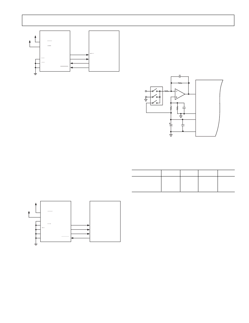
APPL IC AT ION HINT S
Bipolar and Wider Input Ranges
In some applications, it is desired to use a bipolar or wider
analog input range like, for instance, ±10 V, ±5 V or 0 V to 5 V.
Although the AD7667 has only one unipolar range, by simple
modifications of the input driver circuitry, bipolar and wider
input ranges can be used without any performance degradation.
Figure 23 shows a connection diagram which allows
that. C omponents values required and resulting full-
scale ranges are shown in T able II.
For applications where accurate gain and offset are de-
sired, they can be calibrated by acquiring a ground and a
voltage reference using an analog multiplexer, U2, as
shown for bipolar input ranges in Figure 23.
U1
ANALOG
INPUT
R2
R3
R4
100nF
R1
C
F
U2
C
REF
IN
INGND
REF
REFGND
100nF
AD7667
Figure 23. Using the AD7667 in 16-Bit Bipolar and/or
Wider Input Ranges
T able II. Component Values and Input Ranges
Input Range
R1
R2
R3
R4
±10 V
±5 V
0 V to –5 V
250
500
1 k
2 k
2 k
2 k
10 k
10 k
None
8 k
6.67 k
0
L ayout
T he AD7667 has very good immunity to noise on the
power supplies as can be seen in Figure 9. However, care
should still be taken with regard to grounding layout.
T he printed circuit board that houses the AD7667 should be
designed so the analog and digital sections are separated and
confined to certain areas of the board. T his facilitates the use
of ground planes that can be easily separated. Digital and
analog ground planes should be joined in only one place,
preferably underneath the AD7667, or, at least, as close as
possible to the AD7667. If the AD7667 is in a system where
multiple devices require analog-to-digital ground connections,
the connection should still be made at one point only, a star
ground point, which should be established as close as possible
to the AD7667.
It is recommended to avoid running digital lines under
the device as these will couple noise onto the die. T he ana-
log ground plane should be allowed to run under the
AD7667 to avoid noise coupling. Fast switching signals
like
CNVST
or clocks should be shielded with digital
ground to avoid radiating noise to other sections of the
board, and should never run near analog signal paths.
Crossover of digital and analog signals should be avoided.
T races on different but close layers of the board should run
相關PDF資料 |
PDF描述 |
|---|---|
| AD7651ACP | 16-Bit 100 kSPS PulSAR Unipolar ADC with Reference |
| AD7651AST | 16-Bit 100 kSPS PulSAR Unipolar ADC with Reference |
| AD7651ASTRL | 16-Bit 100 kSPS PulSAR Unipolar ADC with Reference |
| AD7654 | Dual 2-Channel Simultaneous Sampling SAR 500 kSPS 16-Bit ADC |
| AD7654ACP | Dual 2-Channel Simultaneous Sampling SAR 500 kSPS 16-Bit ADC |
相關代理商/技術參數 |
參數描述 |
|---|---|
| AD7671ACP | 制造商:Analog Devices 功能描述:ADC Single SAR 1Msps 16-bit Parallel/Serial 48-Pin LFCSP EP 制造商:Rochester Electronics LLC 功能描述:16-BIT, 1MSPS CMOS ADC - Bulk 制造商:Analog Devices 功能描述:Analog Devices AD7671ACP Analog to Digital Converters (ADC) |
| AD7671ACPRL | 制造商:Analog Devices 功能描述:ADC Single SAR 1Msps 16-bit Parallel/Serial 48-Pin LFCSP EP T/R |
| AD7671ACPZ | 功能描述:IC ADC 16BIT CMOS 1MSPS 48LFCSP RoHS:是 類別:集成電路 (IC) >> 數據采集 - 模數轉換器 系列:PulSAR® 其它有關文件:TSA1204 View All Specifications 標準包裝:1 系列:- 位數:12 采樣率(每秒):20M 數據接口:并聯 轉換器數目:2 功率耗散(最大):155mW 電壓電源:模擬和數字 工作溫度:-40°C ~ 85°C 安裝類型:表面貼裝 封裝/外殼:48-TQFP 供應商設備封裝:48-TQFP(7x7) 包裝:Digi-Reel® 輸入數目和類型:4 個單端,單極;2 個差分,單極 產品目錄頁面:1156 (CN2011-ZH PDF) 其它名稱:497-5435-6 |
| AD7671ACPZRL | 功能描述:IC ADC 16BIT CMOS 1MSPS 48LFCSP RoHS:是 類別:集成電路 (IC) >> 數據采集 - 模數轉換器 系列:PulSAR® 標準包裝:1 系列:- 位數:14 采樣率(每秒):83k 數據接口:串行,并聯 轉換器數目:1 功率耗散(最大):95mW 電壓電源:雙 ± 工作溫度:0°C ~ 70°C 安裝類型:通孔 封裝/外殼:28-DIP(0.600",15.24mm) 供應商設備封裝:28-PDIP 包裝:管件 輸入數目和類型:1 個單端,雙極 |
| AD7671AST | 制造商:Analog Devices 功能描述:ADC Single SAR 1Msps 16-bit Parallel/Serial 48-Pin LQFP 制造商:Analog Devices 功能描述:IC 16-BIT ADC |
發布緊急采購,3分鐘左右您將得到回復。