- 您現在的位置:買賣IC網 > PDF目錄373915 > AD7723BS (ANALOG DEVICES INC) 16-Bit, 1.2 MSPS CMOS, Sigma-Delta ADC PDF資料下載
參數資料
| 型號: | AD7723BS |
| 廠商: | ANALOG DEVICES INC |
| 元件分類: | ADC |
| 英文描述: | 16-Bit, 1.2 MSPS CMOS, Sigma-Delta ADC |
| 中文描述: | 1-CH 16-BIT DELTA-SIGMA ADC, SERIAL/PARALLEL ACCESS, PQFP44 |
| 封裝: | MO-112-AA, MQFP-44 |
| 文件頁數: | 18/23頁 |
| 文件大小: | 435K |
| 代理商: | AD7723BS |
AD7723
–18–
REV. 0
Figures 32 and 33 show two such circuits for driving the AD7723.
Figure 32 is intended for use when the input signal is biased
about 2.5 V while Figure 33 is used when the input signal is
biased about ground. While both circuits convert the input
signal into a complementary signal, the circuit in Figure 33
also level shifts the signal so that both outputs are biased
about 2.5 V.
Suitable op amps include the AD8047, AD8044, AD8041 and
its dual equivalent the AD8042. The AD8047 has lower input
noise than the AD8041/42 but has to be supplied from a +7.5 V/
–2.5 V supply. The AD8041/AD8042 will typically degrade
SNR from 90 dB to 88 dB but can be powered from the same
single +5 V supply as the AD7723.
AD8047
AD8047
10k
V
220
V
27
V
220pF
A1
A2
VIN(+)
VIN(–)
REF1
REF2
AD7723
10nF
220nF
220
V
27
V
AIN =
2V
BIASED
ABOUT 2.5V
R
SOURCE
50
V
1
m
F
R
IN
390
V
R
FB
220
V
GAIN = 2
3
R
FB
/(R
SOURCE
+ R
IN
)
Figure 32. Single-Ended to Differential Input Circuit for
Bipolar Mode Operation (Analog Input Biased About +2.5 V)
AD8047
AD8047
R
FB
220
V
220
V
27
V
220pF
A1
A2
VIN(+)
VIN(–)
REF1
REF2
AD7723
10nF
220nF
220
V
27
V
AIN =
6
2V
BIASED
ABOUT
GROUND
1
m
F
R
SOURCE
50
V
R
IN
390
V
R
BALANCE1
220
V
GAIN = 2
3
R
FB
/(R
IN
+ R
SOURCE
)
R
BALANCE1
= R
BALANCE2
3
(R
IN
+ R
SOURCE
)/(2
3
R
FB
)
R
REF2
= R
REF1
3
(R
IN
+ R
SOURCE
)/R
FB
R
REF1
10k
V
R
20k
V
R
BALANCE2
R
BALANCE2
Figure 33. Single-Ended to Differential Input Circuit for
Bipolar Mode Operation (Analog Input Biased About
Ground)
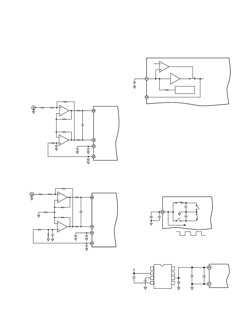
Applying the Reference
The reference circuitry used in the AD7723 includes an on-chip
2.5 V bandgap reference and a reference buffer circuit. The
block diagram of the reference circuit is shown in Figure 34.
The internal reference voltage is connected to REF1 through a
3 k
resistor and is internally buffered to drive the analog
modulator’s switched cap DAC (REF2). When using the inter-
nal reference a 1
μ
F capacitor is required between REF1 and
AGND to decouple the bandgap noise. If the internal reference
is required to bias external circuits, use an external precision op
amp to buffer REF1.
COMPARATOR
REFERENCE
BUFFER
1V
1
m
F
REF2
REF1
2.5V
REFERENCE
SWITCHED-CAP
DAC REFERENCED
AD7723
3k
V
Figure 34. Reference Circuit Block Diagram
Where gain error or gain error drift requires the use of an exter-
nal reference, the reference buffer in Figure 34 can be turned off
by grounding the REF1 pin and the external reference can be
applied directly to pin REF2. The AD7723 will accept an exter-
nal reference voltage between 1.2 V to 3.15 V. By applying a 3 V
rather than a 2.5 V reference, SNR is typically improved by
about 1 dB. Where the output common-mode range of the
amplifier driving the inputs is restricted, the full-scale input
signal span can be reduced by applying a lower than 2.5V refer-
ence. For example, a 1.25 V reference would make the bipolar
input span
±
1 V, but would degrade SNR.
In all cases, since the REF2 voltage connects to the analog
modulator, a 220 nF and 10 nF capacitor must connect directly
from REF2 to AGND. The external capacitor provides the
charge required for the dynamic load presented at the REF2 pin
(See Figure 35).
10nF
220nF
A
B
B
A
4pF
4pF
REF2
SWITCHED-CAP
DAC REFERENCED
CLKIN
A
F
F
F
F
B
A
B
F
F
F
F
Figure 35. REF2 Equivalent Input Circuit
The AD780 is ideal to use as an external reference with the
AD7723. Figure 36 shows a suggested connection diagram.
Grounding Pin 8 on the AD780 selects the 3 V output mode.
1
2
3
4
AD780
AD7723
REF2
REF1
+5V
1
m
F
22nF
220nF
10nF
22
m
F
NC
+V
IN
TEMP
GND
O/P
SELECT
NC
V
OUT
TRIM
2.5V
NC = NO CONNECT
8
7
6
5
Figure 36. External Reference Circuit Connection
相關PDF資料 |
PDF描述 |
|---|---|
| AD7724AST | Dual CMOS Modulators |
| AD7724 | Dual CMOS Modulators |
| AD7725 | 16-Bit 900 kSPS ADC with a Programmable Postprocessor |
| AD7725BS | 16-Bit 900 kSPS ADC with a Programmable Postprocessor |
| AD7729 | Dual Sigma-Delta ADC with Auxiliary DAC |
相關代理商/技術參數 |
參數描述 |
|---|---|
| AD7723BS-REEL | 制造商:Analog Devices 功能描述:Single ADC Delta-Sigma 19.2Msps 16-bit Parallel/Serial 44-Pin MQFP T/R |
| AD7723BSZ | 功能描述:IC ADC 16BIT SIGMA-DELTA 44MQFP RoHS:是 類別:集成電路 (IC) >> 數據采集 - 模數轉換器 系列:- 其它有關文件:TSA1204 View All Specifications 標準包裝:1 系列:- 位數:12 采樣率(每秒):20M 數據接口:并聯 轉換器數目:2 功率耗散(最大):155mW 電壓電源:模擬和數字 工作溫度:-40°C ~ 85°C 安裝類型:表面貼裝 封裝/外殼:48-TQFP 供應商設備封裝:48-TQFP(7x7) 包裝:Digi-Reel® 輸入數目和類型:4 個單端,單極;2 個差分,單極 產品目錄頁面:1156 (CN2011-ZH PDF) 其它名稱:497-5435-6 |
| AD7723BSZ1 | 制造商:AD 制造商全稱:Analog Devices 功能描述:16-Bit, 1.2 MSPS CMOS, Sigma-Delta ADC |
| AD7723BSZ-REEL | 功能描述:IC ADC 16BIT SIGMA-DELTA 44MQFP RoHS:是 類別:集成電路 (IC) >> 數據采集 - 模數轉換器 系列:- 標準包裝:1 系列:- 位數:14 采樣率(每秒):83k 數據接口:串行,并聯 轉換器數目:1 功率耗散(最大):95mW 電壓電源:雙 ± 工作溫度:0°C ~ 70°C 安裝類型:通孔 封裝/外殼:28-DIP(0.600",15.24mm) 供應商設備封裝:28-PDIP 包裝:管件 輸入數目和類型:1 個單端,雙極 |
| AD7723BSZ-REEL1 | 制造商:AD 制造商全稱:Analog Devices 功能描述:16-Bit, 1.2 MSPS CMOS, Sigma-Delta ADC |
發布緊急采購,3分鐘左右您將得到回復。