- 您現在的位置:買賣IC網 > PDF目錄373920 > AD7851 (Analog Devices, Inc.) 14-Bit 333 kSPS Serial A/D Converter PDF資料下載
參數資料
| 型號: | AD7851 |
| 廠商: | Analog Devices, Inc. |
| 英文描述: | 14-Bit 333 kSPS Serial A/D Converter |
| 中文描述: | 14位333 kSPS的串行A / D轉換器 |
| 文件頁數: | 17/36頁 |
| 文件大小: | 435K |
| 代理商: | AD7851 |
第1頁第2頁第3頁第4頁第5頁第6頁第7頁第8頁第9頁第10頁第11頁第12頁第13頁第14頁第15頁第16頁當前第17頁第18頁第19頁第20頁第21頁第22頁第23頁第24頁第25頁第26頁第27頁第28頁第29頁第30頁第31頁第32頁第33頁第34頁第35頁第36頁
–17–
REV. A
AD7851
RE FE RE NCE SE CT ION
For specified performance, it is recommended that when using
an external reference this reference should be between 4 V and
the analog supply AV
DD
. T he connections for the relevant refer-
ence pins are shown in the typical connection diagrams. If the
internal reference is being used, the REF
IN
/REF
OUT
pin should
have a 100 nF capacitor connected to AGND very close to the
REF
IN
/REF
OUT
pin. T hese connections are shown in Figure 18.
If the internal reference is required for use external to the ADC,
it should be buffered at the REF
IN
/REF
OUT
pin and a 100 nF
connected from this pin to AGND. T he typical noise performance
for the internal reference, with 5 V supplies is 150 nV/
√
Hz
@
1 kHz and dc noise is 100
μ
V p-p.
REF
IN
/REF
OUT
AD7851
ANALOG
SUPPLY
+5V
AV
DD
DV
DD
0.01μF
0.1μF
10μF
C
REF1
C
REF2
0.01μF
47nF
0.01μF
470nF
0.1μF
10
Figure 18. Relevant Connections When Using Internal
Reference
T he other option is that the REF
IN
/REF
OUT
pin be overdriven
by connecting it to an external reference. T his is possible due to
the series resistance from the REF
IN
/REF
OUT
pin to the internal
reference. T his external reference can have a range that includes
AV
DD
. When using AV
DD
as the reference source, the 100 nF
capacitor from the REF
IN
/REF
OUT
pin to AGND should be as
close as possible to the REF
IN
/REF
OUT
pin, and also the C
REF1
pin should be connected to AV
DD
to keep this pin at the same
level as the reference. T he connections for this arrangement are
shown in Figure 19. When using AV
DD
it may be necessary to
add a resistor in series with the AV
DD
supply. T his will have the
effect of filtering the noise associated with the AV
DD
supply.
REF
IN
/REF
OUT
AD7851
ANALOG
SUPPLY
+5V
AV
DD
DV
DD
0.01μF
0.1μF
10μF
C
REF1
C
REF2
0.01μF
47nF
0.01μF
470nF
0.1μF
10
10
Figure 19. Relevant Connections When Using AV
DD
as the
Reference
AD7851 PE RFORMANCE CURVE S
Figure 20 shows a typical FFT plot for the AD7851 at 333 kHz
sample rate and 10 kHz input frequency.
FREQUENCY – kHz
0
–20
–120
0
100
20
S
40
60
80
–40
–60
–80
–100
AV
DD
= DV
= 5V
F
SAMPLE
= 333 kHz
F
SNR = 79.5dB
THD = –95.2
Figure 20. FFT Plot
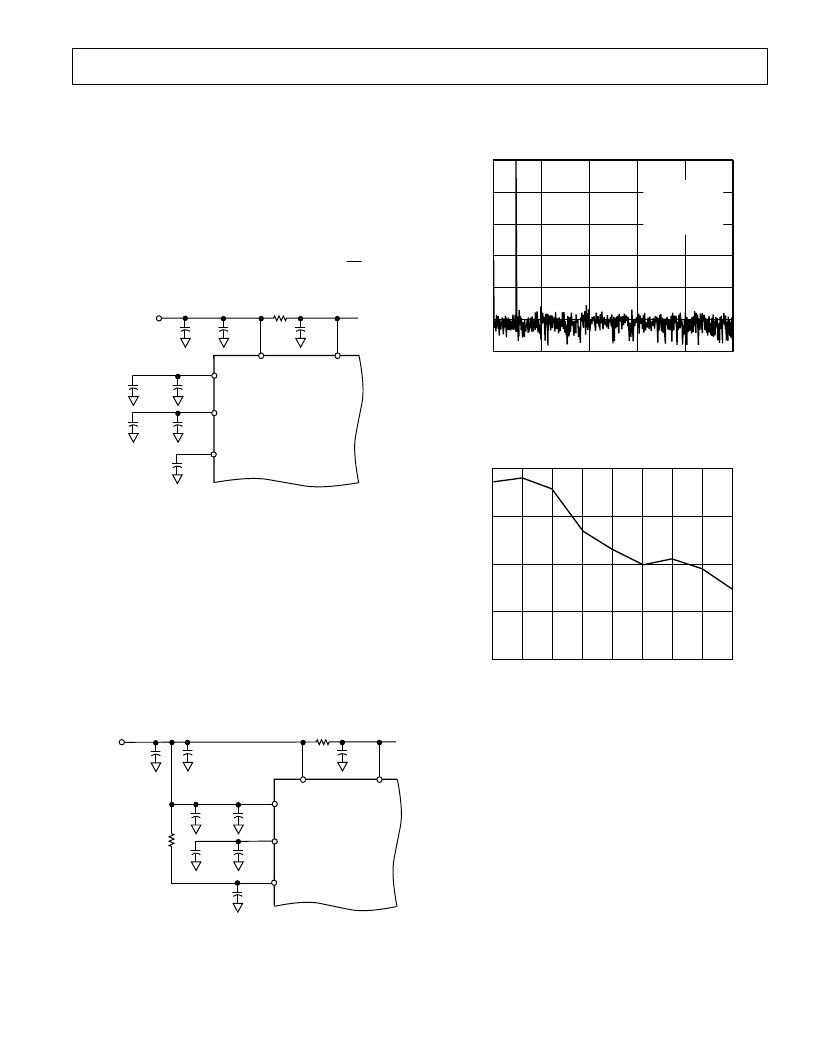
Figure 21 shows the SNR versus Frequency for 5 V supply and
a 4.096 external references (5 V reference is typically 1 dB bet-
ter performance).
INPUT FREQUENCY – kHz
Figure 21. SNR vs. Frequency
Figure 22 shows the Power Supply Rejection Ratio versus
Frequency for the part. T he Power Supply Rejection Ratio is
defined as the ratio of the power in ADC output at frequency f
to the power of a full-scale sine wave.
PSRR (dB) =
10
log (Pf/Pfs)
Pf
= Power at frequency f in ADC output,
Pfs
= power of a full-
scale sine wave. Here a 100 mV peak-to-peak sine wave is
coupled onto the AV
DD
supply while the digital supply is left
unaltered.
79
75
0
166
20
50
120
140
78
77
76
S
10
80
100
相關PDF資料 |
PDF描述 |
|---|---|
| AD7851AN | 14-Bit 333 kSPS Serial A/D Converter |
| AD7851AR | 14-Bit 333 kSPS Serial A/D Converter |
| AD7851ARS | 14-Bit 333 kSPS Serial A/D Converter |
| AD7851KN | 14-Bit 333 kSPS Serial A/D Converter |
| AD7851KR | 14-Bit 333 kSPS Serial A/D Converter |
相關代理商/技術參數 |
參數描述 |
|---|---|
| AD7851AN | 制造商:Analog Devices 功能描述:ADC Single SAR 333ksps 14-bit Serial 24-Pin PDIP 制造商:Rochester Electronics LLC 功能描述:14 BIT SELF CALIBRATION ADC I.C. - Bulk |
| AD7851ANZ | 功能描述:IC ADC 14BIT SRL 333KSPS 24-DIP RoHS:是 類別:集成電路 (IC) >> 數據采集 - 模數轉換器 系列:- 產品培訓模塊:Lead (SnPb) Finish for COTS Obsolescence Mitigation Program 標準包裝:2,500 系列:- 位數:12 采樣率(每秒):3M 數據接口:- 轉換器數目:- 功率耗散(最大):- 電壓電源:- 工作溫度:- 安裝類型:表面貼裝 封裝/外殼:SOT-23-6 供應商設備封裝:SOT-23-6 包裝:帶卷 (TR) 輸入數目和類型:- |
| AD7851AR | 制造商:Analog Devices 功能描述:ADC Single SAR 333ksps 14-bit Serial 24-Pin SOIC W 制造商:Rochester Electronics LLC 功能描述:14 BIT SELF CALIBRATION ADC I.C. - Bulk |
| AD7851AR-REEL | 制造商:Analog Devices 功能描述:ADC Single SAR 333ksps 14-bit Serial 24-Pin SOIC W T/R |
| AD7851ARS | 制造商:Analog Devices 功能描述:ADC Single SAR 333ksps 14-bit Serial 24-Pin SSOP 制造商:Analog Devices 功能描述:IC 14-BIT ADC |
發布緊急采購,3分鐘左右您將得到回復。