- 您現在的位置:買賣IC網 > PDF目錄373945 > AD8370-EVAL (Analog Devices, Inc.) LF to 750 MHz Digitally Controlled VGA PDF資料下載
參數資料
| 型號: | AD8370-EVAL |
| 廠商: | Analog Devices, Inc. |
| 元件分類: | 運動控制電子 |
| 英文描述: | LF to 750 MHz Digitally Controlled VGA |
| 中文描述: | LF到750兆赫數字控制VGA |
| 文件頁數: | 18/28頁 |
| 文件大小: | 1043K |
| 代理商: | AD8370-EVAL |
第1頁第2頁第3頁第4頁第5頁第6頁第7頁第8頁第9頁第10頁第11頁第12頁第13頁第14頁第15頁第16頁第17頁當前第18頁第19頁第20頁第21頁第22頁第23頁第24頁第25頁第26頁第27頁第28頁
AD8370
Rev. 0 | Page 18 of 28
–100
–90
–80
–70
–60
–50
–40
H
0
96
32
64
0
32
64
96
128
GAIN CODE
0
HD2
HD2
LOW GAIN MODE
HIGH GAIN MODE
HD3
HD3
Figure 48. Harmonic Distortion of the Circuit in Figure 45
DC-COUPLED OPERATION
AD8370
I
I
V
P
V
V
O
O
O
O
V
L
C
D
I
I
6
7
8
2
3
5
1
11
10
9
15
14
16
13
12
4
SERIAL CONTROL
INTERFACE
1nF
1nF
0.1
μ
F
0.1
μ
F
–2.5V
–2.5V
0V
0V
+2.5V
R
L
SINGLE-
ENDED
GROUND
REFERENCED
SOURCE
R
S
R
T
0
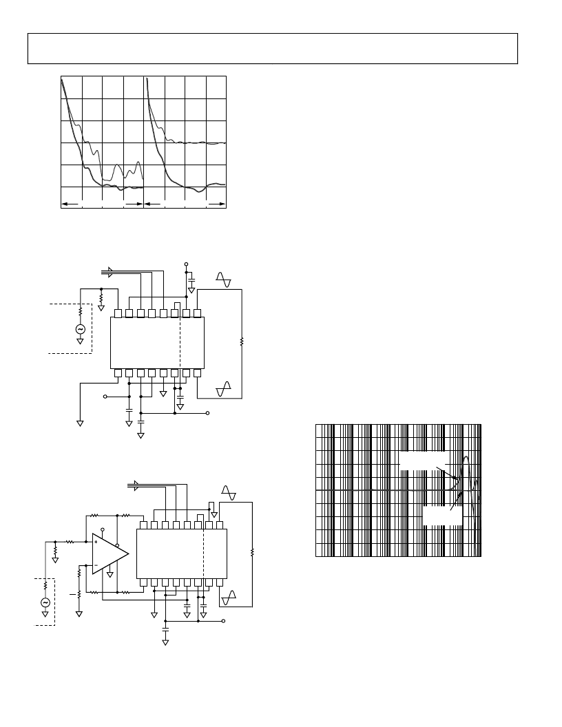
Figure 49. DC Coupling the AD8370. Dual supplies are used to set the input
and output common-mode levels to 0 V.
AD8370
AD8138
I
I
V
P
V
V
O
O
O
O
V
L
C
D
I
I
6
7
8
2
3
5
1
11
10
9
15
14
16
13
12
4
SERIAL CONTROL
INTERFACE
1nF
1nF
0.1
μ
F
+5V
499
499
100
499
499
100
V
O
V
OCM
V
OCM
+5V
R
L
SINGLE-ENDED GROUND
REFERENCED SOURCE
R
S
R
T
R
T
2
0
Figure 50. DC Coupling the AD8370. The AD8138 is used as a unity gain level
shifting amplifier to lift the common-mode level of the source to midsupply.
The AD8370 is also a dc accurate variable gain amplifier. The
common-mode dc voltage present at the output pins is internally
set to midsupply using what is essentially a buffered resistive
divider network connected between the positive supply rail and
the common (ground) pins. The input pins are at a slightly
higher dc potential, typically 250 mV to 550 mV above the out-
put pins, depending on gain setting. In a typical single-supply
application, it is necessary to raise the common-mode reference
level of the source and load to roughly midsupply to maintain
symmetric swing and to avoid sinking or sourcing strong bias
currents from the input and output pins. It is possible to use
balanced dual supplies to allow ground referenced source and
load as indicated in Figure 49. By connecting the VOCM pin
and unused input to ground, the input and output common-
mode potentials are forced to virtual ground. This allows direct
coupling of ground referenced source and loads. The initial
differential input offset is typically only a few 100
μ
V. Over
temperature, the input offset could be as high as a few tens of
mVs. If precise dc accuracy is need over temperature and time, it
may be necessary to periodically measure the input offset and to
apply the necessary opposing offset to the unused differential
input, canceling the resulting output offset.
To address situations where dual supplies are not convenient, a
second option is presented in Figure 50. The AD8138 differential
amplifier is used to translate the common-mode level of the
driving source to midsupply, which allows dc accurate perform-
ance with a ground-referenced source without the need for dual
supplies. The bandwidth of the solution in Figure 50 is limited
by the gain-bandwidth product of the AD8138. The normalized
frequency response of both implementations is shown in Figure 51.
–10
–8
–6
–4
–2
0
2
4
6
8
10
N
1
10
100
1k
10k
100k
1M
10M
100M
1G
FREQUENCY (Hz)
0
AD8370 WITH
AD8138 SINGLE
+5V SUPPLY
AD8370
USING DUAL
±2.5V SUPPLY
Figure 51. Normalized Frequency Response of the Two Solutions in
Figure 49 and Figure 50
相關PDF資料 |
PDF描述 |
|---|---|
| AD8370ARE | LF to 750 MHz Digitally Controlled VGA |
| AD8370ARE-REEL7 | LF to 750 MHz Digitally Controlled VGA |
| AD8383 | Low Cost 10-Bit, 6-Channel Output Decimating LCD DecDriver |
| AD8383ACPZ | Low Cost 10-Bit, 6-Channel Output Decimating LCD DecDriver |
| AD8391 | xDSL Line Driver 3 V to 12 V with Power-Down |
相關代理商/技術參數 |
參數描述 |
|---|---|
| AD8370-EVALZ | 制造商:Analog Devices 功能描述:- Bulk |
| AD8372 | 制造商:AD 制造商全稱:Analog Devices 功能描述:41 dB Range, 1 dB Step Size, Programmable Dual VGA |
| AD8372ACPZ-R7 | 功能描述:IC AMP VGA DIFF DUAL LN 32LFCSP RoHS:是 類別:集成電路 (IC) >> Linear - Amplifiers - Instrumentation 系列:- 標準包裝:2,500 系列:- 放大器類型:通用 電路數:4 輸出類型:- 轉換速率:0.6 V/µs 增益帶寬積:1MHz -3db帶寬:- 電流 - 輸入偏壓:45nA 電壓 - 輸入偏移:2000µV 電流 - 電源:1.4mA 電流 - 輸出 / 通道:40mA 電壓 - 電源,單路/雙路(±):3 V ~ 32 V,±1.5 V ~ 16 V 工作溫度:0°C ~ 70°C 安裝類型:表面貼裝 封裝/外殼:14-TSSOP(0.173",4.40mm 寬) 供應商設備封裝:14-TSSOP 包裝:帶卷 (TR) 其它名稱:LM324ADTBR2G-NDLM324ADTBR2GOSTR |
| AD8372ACPZ-R71 | 制造商:AD 制造商全稱:Analog Devices 功能描述:41 dB Range, 1 dB Step Size, Programmable Dual VGA |
| AD8372ACPZ-WP | 制造商:Analog Devices 功能描述: 制造商:Rochester Electronics LLC 功能描述: |
發布緊急采購,3分鐘左右您將得到回復。