- 您現在的位置:買賣IC網 > PDF目錄373969 > AD9847 (Analog Devices, Inc.) 10-Bit 40 MSPS CCD Signal Processor with Integrated Timing Driver PDF資料下載
參數資料
| 型號: | AD9847 |
| 廠商: | Analog Devices, Inc. |
| 英文描述: | 10-Bit 40 MSPS CCD Signal Processor with Integrated Timing Driver |
| 中文描述: | 10位40 MSPS的CCD信號處理器集成時序驅動 |
| 文件頁數: | 25/28頁 |
| 文件大小: | 428K |
| 代理商: | AD9847 |
第1頁第2頁第3頁第4頁第5頁第6頁第7頁第8頁第9頁第10頁第11頁第12頁第13頁第14頁第15頁第16頁第17頁第18頁第19頁第20頁第21頁第22頁第23頁第24頁當前第25頁第26頁第27頁第28頁
REV. A
AD9847
–25–
Optical Black Clamp
The optical black clamp loop is used to remove residual offsets in
the signal chain and to track low frequency variations in the CCD’s
black level. During the optical black (shielded) pixel interval on
each line, the ADC output is compared with a fixed black level
reference, selected by the user in the clamp level register. The
value can be programmed between 0 LSB and 63.75 LSB with
8-bit resolution. The resulting error signal is filtered to reduce noise,
and the correction value is applied to the ADC input through a
D/A converter. Normally, the optical black clamp loop is turned
on once per horizontal line, but this loop can be updated more
slowly to suit a particular application. If external digital clamping
is used during the post processing, the AD9847 optical black
clamping may be disabled using Bit D2 in the OPRMODE
register. When the loop is disabled, the clamp level register may
still be used to provide programmable offset adjustment.
The CLPOB pulse should be placed during the CCD’s optical
black pixels. It is recommended that the CLPOB pulse duration
be at least 20 pixels wide to minimize clamp noise. Shorter pulse-
widths may be used, but clamp noise may increase, and the
ability to track low frequency variations in the black level will be
reduced. See the section on Horizontal Clamping and Blanking
and also the Applications Information section for timing examples.
A/D Converter
The AD9847 uses a high performance 10-bit ADC architecture,
optimized for high speed and low power. Differential nonlinearity
(DNL) performance is typically better than 0.4 LSB. The ADC
uses a 2 V input range. Better noise performance results from
using a larger ADC full-scale range. See TPC 1 and TPC 2 for
typical linearity and noise performance plots for the AD9847.
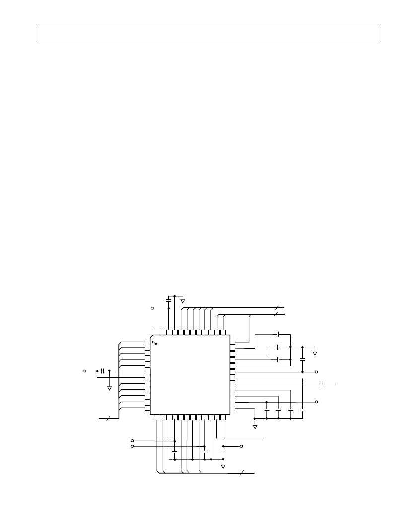
APPLICATIONS INFORMATION
External Circuit Configuration
The AD9847 recommended circuit configuration for external
mode is shown in Figure 21. All signals should be carefully
routed on the PCB to maintain low noise performance. The CCD
output signal should be connected to Pin 29 through a 0.1
μ
F
capacitor. The CCD timing signals H1–H4 and RG should be
routed directly to the CCD with minimum trace lengths, as shown
in Figures 22a and 22b. The digital outputs and clock inputs are
located on Pins 1–12 and Pins 36–44 and should be connected
to the digital ASIC, away from the analog and CCD clock signals.
The CLI signal from the ASIC may be routed under the package
to Pin 23. This will help separate the CLI signal from the H1–H4
and RG signal routing.
Grounding and Decoupling Recommendations
As shown in Figure 21, a single ground plane is recommended
for the AD9847. This ground plane should be as continuous as
possible, particularly around Pins 25 – 35. This will ensure that
all analog decoupling capacitors provide the lowest possible
impedance path between the power and bypass pins and their
respective ground pins. All decoupling capacitors should be located
as close as possible to the package pins. Placing series resistors
close to the digital output pins (Pins 1–12) may help reduce
digital code transition noise. If the digital outputs must drive a
load larger than 20 pF, buffering is recommended to minimize
additional noise.
Power supply decoupling is very important in achieving low noise
performance. Figure 21 shows the local high frequency decoupling
capacitors, but additional capacitance is recommended for lower
frequencies. Additional capacitors and ferrite beads can further
reduce noise.
3V
DIGITAL
SUPPLY
SERIAL
INTERFACE
3
CCD
SIGNAL
CLOCK
INPUTS
6
0.1 F
36
35
34
33
32
31
30
29
28
27
26
25
3V
DRIVER
SUPPLY
13 14 15 16
CLOCK
INPUT
17 18 19 20 21 22 23 24
1
2
RG DRIVER
SUPPLY
3
H DRIVER
SUPPLY
4
5
6
7
8
9
10
11
3V
ANALOG
SUPPLY
12
48 47 46 45 44
39 38 37
43 42 41 40
PIN 1
TOP VIEW
(Not to Scale)
SL
REFT
REFB
CMLEVEL
AVSS3
AVDD3
BYP3
CCDIN
BYP2
BYP1
AVDD2
AVSS2
0.1 F
(LSB) D0
D1
D2
D3
D4
1 F
DVSS3
DVDD3
1 F
D5
D6
D7
D8
AD9847
(MSB) D9
N
N
3V
ANALOG
SUPPLY
D
D
H
V
P
H
C
0.1 F
C
S
S
H
H
D
D
H
H
D
R
D
A
C
A
3V
ANALOG
SUPPLY
DATA
OUTPUTS
10
0.1 F 0.1 F 0.1 F
0.1 F
0.1 F
0.1 F
0.1 F
0.1 F
0.1 F
HIGH-SPEED
CLOCKS
5
Figure 21. Recommended Circuit Configuration for External Mode
相關PDF資料 |
PDF描述 |
|---|---|
| AD9847AKST | 10-Bit 40 MSPS CCD Signal Processor with Integrated Timing Driver |
| AD9848KST | CCD Signal Processors with Integrated Timing Driver |
| AD9848 | CCD Signal Processors with Integrated Timing Driver |
| AD9849 | CCD Signal Processors with Integrated Timing Driver |
| AD9849KST | CCD Signal Processors with Integrated Timing Driver |
相關代理商/技術參數 |
參數描述 |
|---|---|
| AD9847AKCPZ | 制造商:Rochester Electronics LLC 功能描述:- Bulk 制造商:Analog Devices 功能描述: |
| AD9847AKCPZRL | 制造商:Analog Devices 功能描述:DISPLAY DRVR, 10-BIT 40MSPS CCD SGNL PROCESSOR W/ INTEGRATED - Tape and Reel |
| AD9847AKST | 制造商:Analog Devices 功能描述:AFE VID 1ADC 10-BIT 3V/3V/3.3V/3.3V/3.3V/3.3V/3.3V/5V/5V 48L - Trays |
| AD9847AKSTRL | 制造商:Analog Devices 功能描述:AFE Video 1ADC 10-Bit 3.3V/5V 48-Pin LQFP T/R 制造商:Analog Devices 功能描述:AFE VID 1ADC 10-BIT 3V/3V/3.3V/3.3V/3.3V/3.3V/3.3V/5V/5V 48L - Tape and Reel |
| AD9847AKSTZ | 功能描述:IC CCD SIGNAL PROC 10BIT 48-LQFP RoHS:是 類別:集成電路 (IC) >> 接口 - 傳感器和探測器接口 系列:- 其它有關文件:Automotive Product Guide 產品培訓模塊:Lead (SnPb) Finish for COTS Obsolescence Mitigation Program 標準包裝:74 系列:- 類型:觸控式傳感器 輸入類型:數字 輸出類型:數字 接口:JTAG,串行 電流 - 電源:100µA 安裝類型:表面貼裝 封裝/外殼:20-TSSOP(0.173",4.40mm 寬) 供應商設備封裝:20-TSSOP 包裝:管件 |
發布緊急采購,3分鐘左右您將得到回復。