- 您現在的位置:買賣IC網 > PDF目錄373969 > AD9860 (Analog Devices, Inc.) Mixed-Signal Front-End (MxFE⑩) Processor for Broadband Communications PDF資料下載
參數資料
| 型號: | AD9860 |
| 廠商: | Analog Devices, Inc. |
| 英文描述: | Mixed-Signal Front-End (MxFE⑩) Processor for Broadband Communications |
| 中文描述: | 混合寬帶通信信號前端(MxFE⑩)處理器 |
| 文件頁數: | 20/32頁 |
| 文件大小: | 617K |
| 代理商: | AD9860 |
第1頁第2頁第3頁第4頁第5頁第6頁第7頁第8頁第9頁第10頁第11頁第12頁第13頁第14頁第15頁第16頁第17頁第18頁第19頁當前第20頁第21頁第22頁第23頁第24頁第25頁第26頁第27頁第28頁第29頁第30頁第31頁第32頁
REV. 0
–20–
AD9860/AD9862
The second interpolation filter will provide an additional 2 inter-
polation for an overall 4 interpolation. The second filter is a
15 tap filter. It suppresses out-of-band signals by 60 dB or more.
The flat passband response (less than 0.1 dB attenuation) is 38%
of the Tx input data rate (9.5% of f
DAC
). The maximum input
data rate per channel is 32 MSPS per channel when using
4
interpolation.
The 2 and 4 Interpolation Filter Transfer function plots are
shown in Figure 4a and 4b, respectively.
NORMALIZED –
f
S
10
0
M
0
–10
–20
–30
–40
–50
–60
–70
–80
–100
0.1
–90
0.2
0.3
0.4
0.5
0.6
0.7
0.8
0.9
1.0
INTERPOLATION
FILTER
INCLUDUNG SIN (X)/X
NORMALIZED –
f
S
10
0
M
0
–10
–20
–30
–40
–50
–60
–70
–80
–100
0.1
–90
0.2
0.3
0.4
0.5
0.6
0.7
0.8
0.9
1.0
INTERPOLATION
FILTER
INCLUDUNG SIN (X)/X
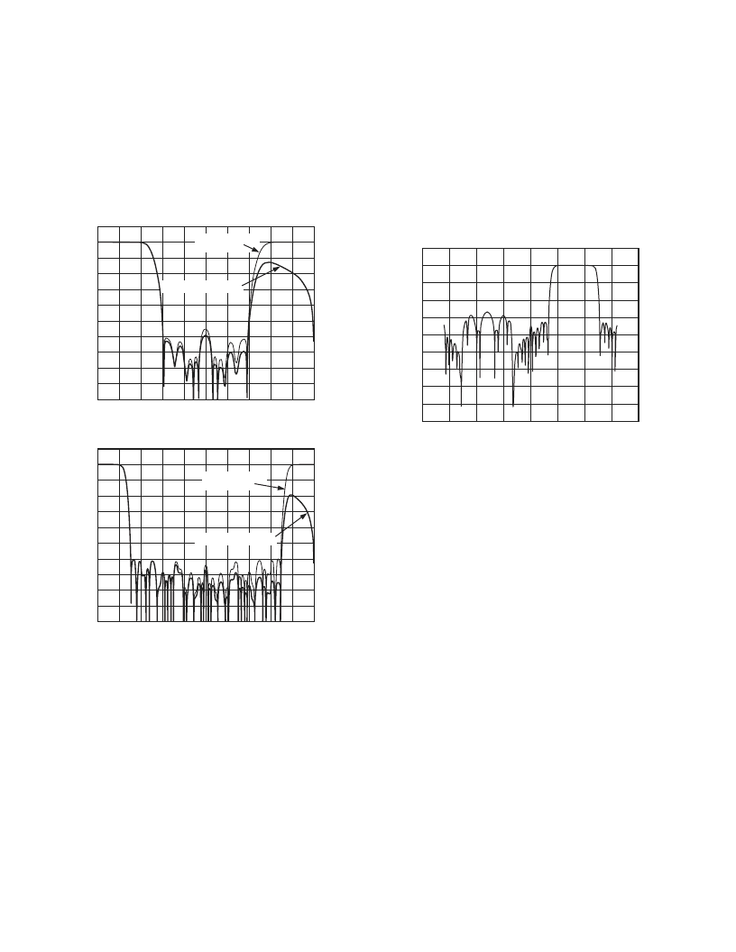
Figure 4. Spectral Response of 2 Interpolation Filter
(top) and 4 Interpolation Filter (bottom)
Fine Modulation Stage
A digital fine modulation stage is available in the transmit path to
shift the complex Tx output spectrum using a 24-bit numerically
controlled oscillator (NCO). To utilize the Fine Modulation
Block, 4 interpolation is required. Therefore, the maximum
input date rate is 32 MSPS per channel, which generates a DAC
update rate, f
DAC
, of 128 MSPS. The NCO can tune up to 1/4 of
f
DAC
, providing a step resolution of f
DAC
/2
26
. Since the Fine
Modulation Stage precedes the Interpolation Filters, care must
be taken to ensure the entire desired signal is placed within the
pass band of the Interpolation Filter.
By default, the Fine Modulation Block is bypassed. To enable it
to perform a complex mix of the Tx I and Q data, Register 2
’
s data
paths, Fine Mod and Fine, should be configured. The NCO
frequency tuning word is set in the three FTW registers.
Hilbert Filter
The Hilbert filter is available to provide a Hilbert transform of
“
real
”
input data at a low intermediate frequency (IF) between
12.5% to 38% of the input data rate. The Hilbert filter essentially
transforms this
“
real,
”
single channel input data into a complex
representation (i.e., I and Q components) that can be used as
part of an image rejection architecture. The complex data can than
be processed further using the on-chip digital complex modulators.
The Hilbert filter requires 4 interpolation to be enabled and
accepts data at a maximum 32 MSPS. Figure 5 shows a spectral
plot of the Hilbert filter impulse response.
FREQUENCY – MHz
100
–20
d
80
60
40
20
0
–20
–40
–60
–80
–100
–15
–10
–5
0
5
10
15
20
Figure 5. Tx Hilbert Filter, Keeping Positive
Frequencies Spectral Plot
Latch/Demultiplexer
The AD9860/AD9862 Tx path accepts dual or single channel
data. The dual channel data can represent two independent real
signals or a complex signal. Various input data latching schemes
relative to one of the output clocks, CLKOUT1 or CLKOUT2,
are allowed, including using any combination of rising and falling
clock edges.
Associated Tx timing is discussed in detail in the Clock Overview
section of the data sheet.
TRANSMIT APPLICATIONS SECTION
The AD9860/AD9862 transmit path (Tx) includes two, high speed,
high performance, 12-/14-bit TxDACs. Figure 3 shows a detailed
block diagram of the transmit data path and can be referred to
throughout the explanation of the various modes of operation.
The various Tx modes of operation are broken into three parts,
determined by the format of the input data. They are:
1. Single Channel DAC Data
2. Two Independent Real Signal DAC Data (diversity or dual
channel
3. Dual Channel Complex DAC Data (I and Q or Single Sideband)
Single Channel DAC Data
In this mode, 12-/14-bit single channel Tx data is provided to
the AD9860/AD9862 and latched using either CLKOUT1 or
CLKOUT2 edges as defined in the Clock Overview section of
the data sheet. All Tx digital signal processing blocks can be
utilized to address reconstruction filtering at the DAC output
and aid in frequency tuning.
相關PDF資料 |
PDF描述 |
|---|---|
| AD9860BST | Mixed-Signal Front-End (MxFE⑩) Processor for Broadband Communications |
| AD9860PCB | Mixed-Signal Front-End (MxFE⑩) Processor for Broadband Communications |
| AD9862 | Mixed-Signal Front-End (MxFE⑩) Processor for Broadband Communications |
| AD9862BST | Mixed-Signal Front-End (MxFE⑩) Processor for Broadband Communications |
| AD9864 | IF Digitizing Subsystem |
相關代理商/技術參數 |
參數描述 |
|---|---|
| AD9860BST | 制造商:Analog Devices 功能描述:Mixed Signal Front End 128-Pin LQFP 制造商:Rochester Electronics LLC 功能描述:10B MIXED SIGNAL FRONT END MXFE PROCESSO - Tape and Reel |
| AD9860BSTRL | 制造商:Analog Devices 功能描述:Mixed Signal Front End 128-Pin LQFP T/R 制造商:Rochester Electronics LLC 功能描述:10B MIXED SIGNAL FRONT END MXFE PROCESSO - Tape and Reel |
| AD9860BSTZ | 功能描述:IC PROCESSOR FRONT END 128LQFP RoHS:是 類別:RF/IF 和 RFID >> RF 前端 (LNA + PA) 系列:- 產品培訓模塊:Lead (SnPb) Finish for COTS Obsolescence Mitigation Program 標準包裝:250 系列:- RF 型:GPS 頻率:1575.42MHz 特點:- 封裝/外殼:48-TQFP 裸露焊盤 供應商設備封裝:48-TQFP 裸露焊盤(7x7) 包裝:托盤 |
| AD9860BSTZRL | 功能描述:IC PROCESSOR FRONT END 128LQFP RoHS:是 類別:RF/IF 和 RFID >> RF 前端 (LNA + PA) 系列:- 產品培訓模塊:Lead (SnPb) Finish for COTS Obsolescence Mitigation Program 標準包裝:250 系列:- RF 型:GPS 頻率:1575.42MHz 特點:- 封裝/外殼:48-TQFP 裸露焊盤 供應商設備封裝:48-TQFP 裸露焊盤(7x7) 包裝:托盤 |
| AD9860-EB | 制造商:Analog Devices 功能描述: |
發布緊急采購,3分鐘左右您將得到回復。