- 您現在的位置:買賣IC網 > PDF目錄373969 > AD9860 (Analog Devices, Inc.) Mixed-Signal Front-End (MxFE⑩) Processor for Broadband Communications PDF資料下載
參數資料
| 型號: | AD9860 |
| 廠商: | Analog Devices, Inc. |
| 英文描述: | Mixed-Signal Front-End (MxFE⑩) Processor for Broadband Communications |
| 中文描述: | 混合寬帶通信信號前端(MxFE⑩)處理器 |
| 文件頁數: | 30/32頁 |
| 文件大小: | 617K |
| 代理商: | AD9860 |
第1頁第2頁第3頁第4頁第5頁第6頁第7頁第8頁第9頁第10頁第11頁第12頁第13頁第14頁第15頁第16頁第17頁第18頁第19頁第20頁第21頁第22頁第23頁第24頁第25頁第26頁第27頁第28頁第29頁當前第30頁第31頁第32頁
REV. 0
–30–
AD9860/AD9862
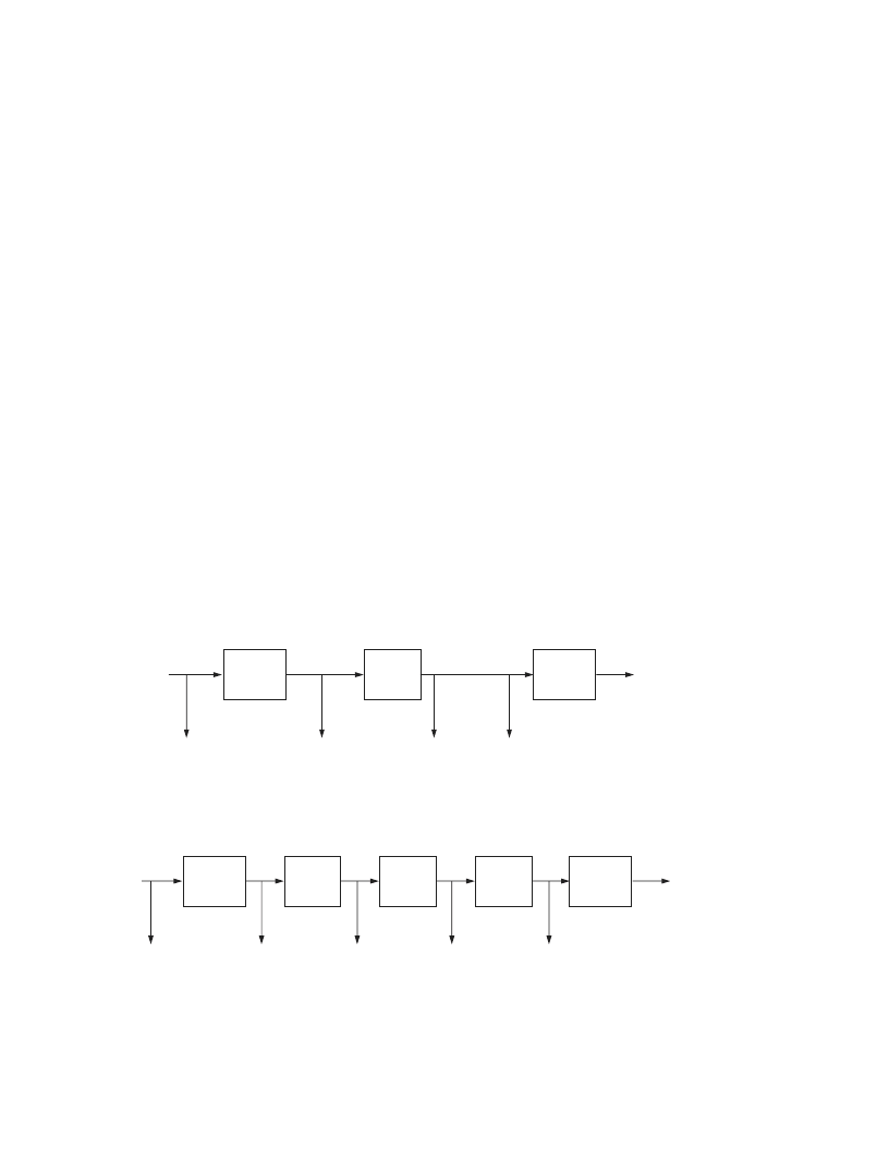
The timing block diagrams in Figures 14 and 15 show how the
various clocks of the single and dual Tx path are affected by the
various register settings.
For dual Tx data, an option to redirect demultiplexed data to
either path is available. For example, the AD9860/AD9862 can
accept complex data in the form of I then Q data or Q then I data,
controlled through QI Order register.
For the dual Tx data cases, the Tx_SYNC pin input logic level
defines what data is currently on the Tx data bus. By default, when
Tx_SYNC is low, Channel A data (first of the set) should be on the
data bus. If TxSYNC is high, Channel B data (or the second of
the set) should be on the Tx bus. This can be reversed by setting
the Inv TxSYNC register.
ADDITIONAL FEATURES
In addition to the features mentioned above in the transmit,
receive and clock paths, the AD9860/AD9862 also integrates
components typically required in communication systems. These
components include auxiliary analog-to-digital converters (AUX
ADC), auxiliary digital-to-analog converters (AUX DAC), and
a sigma-delta output.
Auxiliary ADC
Two auxiliary 10-bit SAR ADCs are available for various external
signals throughout the system, such as a Receive Signal Strength
Indicator (RSSI) function or Temperature Indicator. The auxil-
iary ADCs can convert at rates up to 1.25 MSPS and have a
bandwidth of around 200 kHz. The two auxiliary ADCs (AUX
ADC A and AUX ADC B) have multiplexed inputs, so that up
to four system signals can be monitored.
00: B = A
01: B = 2 A
10: B = 4 A
00: C = B
01: C = B/2
10: C = B/4
00: D = C
01: D = 2 C
10: D = 4 C
ADC SAMPLE RATE
(NOT TO EXCEED 64MHz)
DLL OUTPUT RATE
(NOT TO EXCEED 128MHz)
CLKOUT2
INPUT Tx DATA RATE
(SINGLE CHANNEL)
TxDAC UPDATE RATE
SINGLE CHANNEL
(CANNOT EXCEED
DLL OUTPUT RATE)
CLKIN
A
B
C
D
DLL MULT
CLKOUT2 DIV
INTERP
Figure 14. Single Tx Timing Block Diagram, Alternative Operation
00: B = A
01: B = 2 A
10: B = 4 A
00: C = B
01: C = B/2
10: C = B/4
00: F = G
01: F = 2 G
10: F = 4 G
CLKOUT2
INPUT
Tx DATA RATE
TxDAC UPDATE RATE
EACH CHANNEL
(CANNOT EXCEED
DLL OUTPUT RATE)
CLKIN
A
B
E
F
DLL MULT
CLKOUT2 DIV
INTERP
0: D = C
1: D = 2 C
C
2 EDGES
E = D/2
D
DUAL CHANNEL
FACTOR
ADC SAMPLE RATE
(NOT TO EXCEED 64MHz)
DLL OUTPUT RATE
(NOT TO EXCEED 128MHz)
INPUT Tx DATA RATE
EACH CHANNEL
Figure 15. Dual Tx Timing Block Diagram, Alternative Operation
The AUX ADC A multiplexer controls whether pin AUX_ADC_A1
or pin AUX_ADC_A2 is connected to the input of Auxiliary
ADC A. The multiplexer is programmed through Register D34
B1, SelectA. By default, the register is low, which connects the
AUX_ADC_A2 Pin to the input. Similarly, AUX ADC B has a
multiplexed input controlled by Register D34 B4, SelectB. The
default setting for SelectB is low, which connects the AUX_ADC_B2
input pin to AUX ADC B. If the SelectA or SelectB register bit
is set high, then the AUX_ADC_A1 Pin or the AUX_ADC_B1
pin is connected to the respective AUX ADC input.
An internal reference buffer provides a full-scale reference for
both of the auxiliary ADCs that is equal to the supply voltage for
the auxiliary ADCs. An external full-scale reference can be applied
to either or both of the AUX ADCs by setting the appropriate
bit(s), RefselB for the AUX ADC B and Refsel A for the AUX
ADC B in the Register Map. Setting either or both of these bits
high will disconnect the internal reference buffer and enable the
externally applied reference from the AUX_REF Pin to the
respective channel(s).
Timing for the auxiliary ADCs is generated from a divided down
Rx ADC clock. The divide down ratio is controlled by register
D35 B0, CLK/4 and is used to maintain a maximum clock rate of
20 MHz. By default, CLK/4 is set low dividing the Rx ADC clock
by 2; this is acceptable when running the Rx ADC at rate of
40 MHz or less. At Rx ADC rate greater than 40 MHz, the CLK/4
register bit should be set high and will divide the Rx ADC clock
by 4 to derive the auxiliary ADC Clock. The conversion time,
including setup, takes 16 clock cycles (16 Rx ADC clock cycles);
when CLK/4 is set low, divide by 2 mode, or 32 clock cycles
when CLK/4 is set high.
相關PDF資料 |
PDF描述 |
|---|---|
| AD9860BST | Mixed-Signal Front-End (MxFE⑩) Processor for Broadband Communications |
| AD9860PCB | Mixed-Signal Front-End (MxFE⑩) Processor for Broadband Communications |
| AD9862 | Mixed-Signal Front-End (MxFE⑩) Processor for Broadband Communications |
| AD9862BST | Mixed-Signal Front-End (MxFE⑩) Processor for Broadband Communications |
| AD9864 | IF Digitizing Subsystem |
相關代理商/技術參數 |
參數描述 |
|---|---|
| AD9860BST | 制造商:Analog Devices 功能描述:Mixed Signal Front End 128-Pin LQFP 制造商:Rochester Electronics LLC 功能描述:10B MIXED SIGNAL FRONT END MXFE PROCESSO - Tape and Reel |
| AD9860BSTRL | 制造商:Analog Devices 功能描述:Mixed Signal Front End 128-Pin LQFP T/R 制造商:Rochester Electronics LLC 功能描述:10B MIXED SIGNAL FRONT END MXFE PROCESSO - Tape and Reel |
| AD9860BSTZ | 功能描述:IC PROCESSOR FRONT END 128LQFP RoHS:是 類別:RF/IF 和 RFID >> RF 前端 (LNA + PA) 系列:- 產品培訓模塊:Lead (SnPb) Finish for COTS Obsolescence Mitigation Program 標準包裝:250 系列:- RF 型:GPS 頻率:1575.42MHz 特點:- 封裝/外殼:48-TQFP 裸露焊盤 供應商設備封裝:48-TQFP 裸露焊盤(7x7) 包裝:托盤 |
| AD9860BSTZRL | 功能描述:IC PROCESSOR FRONT END 128LQFP RoHS:是 類別:RF/IF 和 RFID >> RF 前端 (LNA + PA) 系列:- 產品培訓模塊:Lead (SnPb) Finish for COTS Obsolescence Mitigation Program 標準包裝:250 系列:- RF 型:GPS 頻率:1575.42MHz 特點:- 封裝/外殼:48-TQFP 裸露焊盤 供應商設備封裝:48-TQFP 裸露焊盤(7x7) 包裝:托盤 |
| AD9860-EB | 制造商:Analog Devices 功能描述: |
發布緊急采購,3分鐘左右您將得到回復。