- 您現在的位置:買賣IC網 > PDF目錄373969 > AD9860 (Analog Devices, Inc.) Mixed-Signal Front-End (MxFE⑩) Processor for Broadband Communications PDF資料下載
參數資料
| 型號: | AD9860 |
| 廠商: | Analog Devices, Inc. |
| 英文描述: | Mixed-Signal Front-End (MxFE⑩) Processor for Broadband Communications |
| 中文描述: | 混合寬帶通信信號前端(MxFE⑩)處理器 |
| 文件頁數: | 23/32頁 |
| 文件大小: | 617K |
| 代理商: | AD9860 |
第1頁第2頁第3頁第4頁第5頁第6頁第7頁第8頁第9頁第10頁第11頁第12頁第13頁第14頁第15頁第16頁第17頁第18頁第19頁第20頁第21頁第22頁當前第23頁第24頁第25頁第26頁第27頁第28頁第29頁第30頁第31頁第32頁
REV. 0
AD9860/AD9862
–23–
from each to ground. The internal references can also be disabled
(powered down) and driven externally to provide a different input
voltage range or low drift reference. If an external V
REF
reference
is used, it should not exceed 1.0 V.
A Shared Reference mode allows the user to connect the differen-
tial references from both ADCs together externally for superior
gain matching performance. If the ADCs are to function inde-
pendently, then the reference can be left separate and will provide
superior isolation between the dual channels. Shared Reference
mode can be enabled through the Shared Ref register.
A power-down option allows the user to power down both ADCs
(sleep mode) or either ADC individually to reduce power
consumption.
Decimation Stage
For signals with maximum frequencies less than or equal to 3/16 the
ADC sampling rate, f
ADC
, the decimate by 2 filter (or half-band
filter) can be used to provide on-chip suppression of out-of- band
images and noise. When data is present in frequencies greater
than 1/4 f
ADC
, the decimate by 2 filter can be disabled by switching
the filter out of the circuit. The decimation filter allows the ADC
to oversample the input while decreasing the output data rate by
half. The two main benefits are a simplification of the input anti-
aliasing filter and a slower data interface rate with the external
digital ASIC. The decimation filter is an 11 tap filter and suppresses
out of band noise by 38 dB.
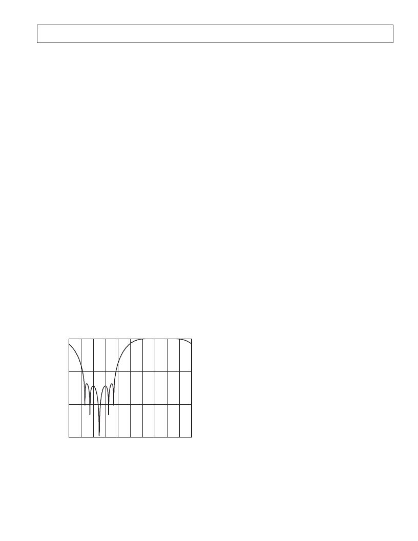
Hilbert Block
The Hilbert filter is available to provide a Hilbert Transform of the
data from the ADC in Channel B. The Digital Hilbert Transform,
in combination with an external complex downconverter, enables
a receive image rejection architecture (similar to Hartley image
rejection architecture). The Hilbert filter pass-band (< 0.1 dB
ripple) is between 25% to 75% of the Nyquist rate of its input data
rate. The maximum data rate of the Rx Hilbert filter is 32 MSPS.
At ADC rates higher than this, the decimation filters should be
enabled. The Hilbert filter transfer function plots are shown in
Figure 7.
NORMALIZED –
f
S
–40
–0.5
M
–80
–120
–0.4
–0.3
–0.2
–0.1
0
0.1
0.2
0.3
0.4
0.5
0
Figure 7. Rx Hilbert Filter, Keeping Positive Frequencies
Response
Data Output Multiplexer Stage
The Rx data output format can be configured for either twos
complement or offset binary. This is controlled by the Rx Twos
Complement register.
The output data from the dual ADCs can be multiplexed onto
a single 10-/12-bit output bus. The multiplexing is synchronized
using the RxSYNC output pin that indicates which channel data
is on the output bus.
RECEIVE APPLICATIONS SECTION
The AD9860/AD9862 receive path (Rx) includes two high speed,
high performance, 10-/12-bit ADCs. Figure 6 shows a detailed
block diagram of the Rx data path and can be referred to through-
out the explanation of the various modes of operation. The various
Rx modes of operation are broken into three parts determined by
the type of input signal:
1. Single Channel ADC Signal
2. Dual Channel Real ADC Signal (diversity or dual channel)
3. Dual Channel Complex ADC Signal (I and Q or Single
Sideband).
Each one of these parts is further divided into two cases, sampling
input signals up to Nyquist of the ADC (Nyquist sampling) and
sampling at rates above ADC Nyquist rate (IF sampling or
undersampling).
The AD9860/AD9862 uses oversampling and decimation filters to
ease requirements on external filtering components. The decima-
tion filters (for both receive paths) can be used or bypassed so as
to accommodate different signal bandwidths and provide different
output data rates to allow easy integration with several different
data processing schemes.
Nonbaseband data can be used in an effort to avoid the dc offsets
in the receive signal path that can cause errors. By receiving
nonbaseband data, the requirements of external filtering may be
greatly reduced.
In each of the different receive modes, the input buffer, Program-
mable Gain Amplifier (RxPGA), and output multiplexer remain
within the receive path.
Single Channel ADC Signal
In this mode, a single input signal to be digitized is connected to
the differential input pins, VIN+A and VIN
–
A. The 10-/12-bit
output Rx data is latched using either CLKOUT1 or CLKOUT2
edges as defined in the Clock Overview section. The Rx path
available options include bypassing the input buffer, Rx PGA
control and using the Decimation Filter. By default, both Rx paths
are enabled and the unused one should be powered down using
the appropriate bit in the Rx Power-Down register, d1.
The input buffer description above explains the conditions under
which the buffer should be bypassed.
If the input signal, or the undersampled alias signal for the
IF sampling case, falls below 40% of the ADC Nyquist rate, the
decimation filter can be enabled to suppress out-of-band noise and
spurious signals by 40 dB or more. With the decimation filter
enabled, the SNR of the Rx path improves by about 2.3 dB.
Dual Channel Real ADC Signal
The Dual Channel Real ADC Signal mode is used to receive
diversity signals or dual independent channel signals that will be
processed independent of each other. In this mode, the two input
signals to be digitized are connected to the differential input pins
of the AD9860/AD9862, VIN+A, VIN
–
A, VIN+B, and VIN
–
B.
The two 10-/12-bit Rx outputs can be either interleaved onto a
single 10-/12-bit bus or output in parallel on two 10-/12-bit buses.
相關PDF資料 |
PDF描述 |
|---|---|
| AD9860BST | Mixed-Signal Front-End (MxFE⑩) Processor for Broadband Communications |
| AD9860PCB | Mixed-Signal Front-End (MxFE⑩) Processor for Broadband Communications |
| AD9862 | Mixed-Signal Front-End (MxFE⑩) Processor for Broadband Communications |
| AD9862BST | Mixed-Signal Front-End (MxFE⑩) Processor for Broadband Communications |
| AD9864 | IF Digitizing Subsystem |
相關代理商/技術參數 |
參數描述 |
|---|---|
| AD9860BST | 制造商:Analog Devices 功能描述:Mixed Signal Front End 128-Pin LQFP 制造商:Rochester Electronics LLC 功能描述:10B MIXED SIGNAL FRONT END MXFE PROCESSO - Tape and Reel |
| AD9860BSTRL | 制造商:Analog Devices 功能描述:Mixed Signal Front End 128-Pin LQFP T/R 制造商:Rochester Electronics LLC 功能描述:10B MIXED SIGNAL FRONT END MXFE PROCESSO - Tape and Reel |
| AD9860BSTZ | 功能描述:IC PROCESSOR FRONT END 128LQFP RoHS:是 類別:RF/IF 和 RFID >> RF 前端 (LNA + PA) 系列:- 產品培訓模塊:Lead (SnPb) Finish for COTS Obsolescence Mitigation Program 標準包裝:250 系列:- RF 型:GPS 頻率:1575.42MHz 特點:- 封裝/外殼:48-TQFP 裸露焊盤 供應商設備封裝:48-TQFP 裸露焊盤(7x7) 包裝:托盤 |
| AD9860BSTZRL | 功能描述:IC PROCESSOR FRONT END 128LQFP RoHS:是 類別:RF/IF 和 RFID >> RF 前端 (LNA + PA) 系列:- 產品培訓模塊:Lead (SnPb) Finish for COTS Obsolescence Mitigation Program 標準包裝:250 系列:- RF 型:GPS 頻率:1575.42MHz 特點:- 封裝/外殼:48-TQFP 裸露焊盤 供應商設備封裝:48-TQFP 裸露焊盤(7x7) 包裝:托盤 |
| AD9860-EB | 制造商:Analog Devices 功能描述: |
發布緊急采購,3分鐘左右您將得到回復。