- 您現在的位置:買賣IC網 > PDF目錄373969 > AD9864BCPZ (ANALOG DEVICES INC) IF Digitizing Subsystem PDF資料下載
參數資料
| 型號: | AD9864BCPZ |
| 廠商: | ANALOG DEVICES INC |
| 元件分類: | 消費家電 |
| 英文描述: | IF Digitizing Subsystem |
| 中文描述: | SPECIALTY CONSUMER CIRCUIT, QCC48 |
| 封裝: | LEAD FREE, MO-220VKKD-2, LFCSP-48 |
| 文件頁數: | 26/44頁 |
| 文件大?。?/td> | 1984K |
| 代理商: | AD9864BCPZ |
第1頁第2頁第3頁第4頁第5頁第6頁第7頁第8頁第9頁第10頁第11頁第12頁第13頁第14頁第15頁第16頁第17頁第18頁第19頁第20頁第21頁第22頁第23頁第24頁第25頁當前第26頁第27頁第28頁第29頁第30頁第31頁第32頁第33頁第34頁第35頁第36頁第37頁第38頁第39頁第40頁第41頁第42頁第43頁第44頁
AD9864
Table 13. SPI Registers Associated with CLK Synthesizer
Address
(Hex)
Breakdown
0x00
(7:0)
0x01
(3:2)
0x10
(5:0)
0x11
(7:0)
0x12
(4:0)
0x13
(7:0)
0x14
(6)
(5)
(4:2)
(1:0)
0x15
(3:0)
0x16
(7:0)
FREQUENCY (MHz)
500
100
400
600
200
R
)
0
550
450
150
50
350
300
350
300
250
0
Bit
Width
8
2
6
8
5
8
1
1
3
1
4
8
Default
Value
0xFF
0
00
0x38
0x00
0x3C
0
0
0
0
0x0
0x04
Name
STBY
CKOB
CKR (13:8)
CKR (7:0)
CKN (12:8)
CKN (7:0)
CKF
CKINV
CKI
CKTM
CKFA (13:8)
CKFA (7:0)
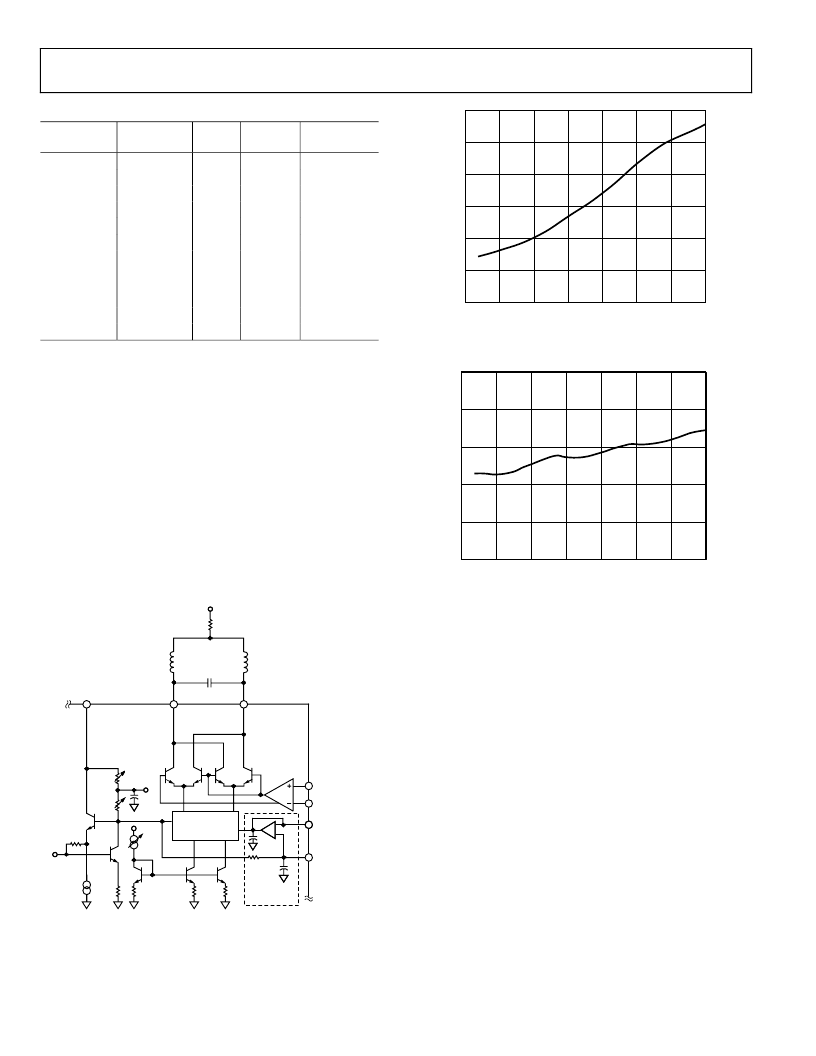
Figure 44. The Shunt Input Resistance vs.
the Frequency of the AD9864’s IF1 Input
FREQUENCY (MHz)
1.5
100
0.5
2.5
200
C
0
2.0
1.0
150
50
0
350
300
250
0
IF LNA/MIXER
The AD9864 contains a single-ended LNA followed by a Gil-
bert-type active mixer, shown in Figure 43 with the required
external components. The LNA uses negative shunt feedback to
set its input impedance at the IFIN pin, thus making it depend-
ent on the input frequency. It can be modeled as approximately
370 ||1.4 pF (±20%) below 100 MHz. Figure 44 and Figure 45
show the equivalent input impedance versus frequency charac-
teristics of the AD9864. The increase in shunt resistance versus
frequency can be attributed to the reduction in bandwidth, thus
the amount of negative feedback of the LNA. Note that the
input signal into IFIN should be ac-coupled via a 10 nF capaci-
tor since the LNA input is self-biasing.
Figure 45. The Shunt Capacitance vs. the Frequency of the AD9864’s IF1 Input
IFIN
R
BIAS
VDDI
MXOP
LO INPUT =
0.3V p-p TO
1.0V p-p
DC SERVO
LOOP
MULTI-TANH
V–I STAGE
CXIF
MXON
CXVM
C
L
L
CXVL
2.7V TO 3.6V
R
GAIN
R
F
0
50
The mixer’s differential LO port is driven by the LO buffer
stage shown in Figure 43, which can be driven single-ended or
differential. Since it is self-biasing, the LO signal level can be
ac-coupled and range from 0.3 V p-p to 1.0 V p-p with negligi-
ble effect on performance. The mixer’s open-collector outputs,
MXOP and MXON, drive an external resonant tank consisting
of a differential LC network tuned to the IF of the band-pass
Σ- ADC, i.e., f
IF2_ADC
= f
CLK
/8. The two inductors provide a dc
bias path for the mixer core via a series resistor of 50 , which
is included to dampen the common-mode response. The
mixer’s output must be ac-coupled to the input of the band-
pass Σ- ADC, IF2P, and IF2N via two 100 pF capacitors to
ensure proper tuning of the LC center frequency.
The external differential LC tank forms the resonant element for
the first resonator of the band-pass Σ- modulator, and so must
be tuned to the
f
CLK
/8
center frequency of the modulator. The
inductors should be chosen such that their impedance at
f
CLK
/8
is
about 140, i.e., L = 180/
f
CLK
. An accuracy of 20% is considered to
be adequate. For example, at
f
CLK
= 18 MHz, L = 10 μH is a good
choice. Once the inductors have been selected, the required tank
capacitance may be calculated using the relation
Figure 43. Simplified Schematic of AD9864’s LNA/Mixer
Rev. 0 | Page 26 of 44
相關PDF資料 |
PDF描述 |
|---|---|
| AD9864BCPZRL | IF Digitizing Subsystem |
| AD9866BCPRL | Broadband Modem Mixed Signal Front End |
| AD9866CHIPS | Broadband Modem Mixed Signal Front End |
| AD9866 | Broadband Modem Mixed Signal Front End |
| AD9866-EB | Broadband Modem Mixed Signal Front End |
相關代理商/技術參數 |
參數描述 |
|---|---|
| AD9864BCPZ | 制造商:Analog Devices 功能描述:IC, IF SUBSYSTEM, 16-24BIT, 6.8KHZ-270KH |
| AD9864BCPZRL | 功能描述:IC IF SUBSYSTEM GEN-PURP 48LFCSP RoHS:是 類別:RF/IF 和 RFID >> RF 前端 (LNA + PA) 系列:- 產品培訓模塊:Lead (SnPb) Finish for COTS Obsolescence Mitigation Program 標準包裝:250 系列:- RF 型:GPS 頻率:1575.42MHz 特點:- 封裝/外殼:48-TQFP 裸露焊盤 供應商設備封裝:48-TQFP 裸露焊盤(7x7) 包裝:托盤 |
| AD9864-EB | 制造商:Analog Devices 功能描述: |
| AD9864-EBZ | 功能描述:BOARD EVAL FOR AD9864 制造商:analog devices inc. 系列:- 零件狀態:有效 類型:數字轉換器 頻率:10MHz ~ 300MHz 配套使用產品/相關產品:AD9864 所含物品:板 標準包裝:1 |
| AD9865 | 制造商:AD 制造商全稱:Analog Devices 功能描述:Broadband Modem Mixed-Signal Front End |
發布緊急采購,3分鐘左右您將得到回復。