- 您現在的位置:買賣IC網 > PDF目錄373969 > AD9866 (Analog Devices, Inc.) Broadband Modem Mixed Signal Front End PDF資料下載
參數資料
| 型號: | AD9866 |
| 廠商: | Analog Devices, Inc. |
| 英文描述: | Broadband Modem Mixed Signal Front End |
| 中文描述: | 寬帶調制解調器混合信號前端 |
| 文件頁數: | 1/48頁 |
| 文件大小: | 1647K |
| 代理商: | AD9866 |
當前第1頁第2頁第3頁第4頁第5頁第6頁第7頁第8頁第9頁第10頁第11頁第12頁第13頁第14頁第15頁第16頁第17頁第18頁第19頁第20頁第21頁第22頁第23頁第24頁第25頁第26頁第27頁第28頁第29頁第30頁第31頁第32頁第33頁第34頁第35頁第36頁第37頁第38頁第39頁第40頁第41頁第42頁第43頁第44頁第45頁第46頁第47頁第48頁
Broadband Modem Mixed Signal Front End
AD9866
FEATURES
Low cost 3.3 V CMOS MxFE
TM
for broadband modems
12-bit D/A converter
2×/4× interpolation filter
200 MSPS DAC update rate
Integrated 23 dBm line driver with 19.5 dB gain control
12-bit, 80 MSPS A/D converter
12 dB to +48 dB low noise RxPGA (< 2.5 nV/rtHz)
Third order programmable low-pass filter
Flexible digital data path interface
Half- and full-duplex operation
Backward compatible with AD9975 and AD9876
Various power-down/reduction modes
Internal clock multiplier (PLL)
2 auxiliary programmable clock outputs
Available in 64-lead chip scale package or bare die
APPLICATIONS
Powerline networking
VDSL and HPNA
Rev.
0
Information furnished by Analog Devices is believed to be accurate and reliable.
However, no responsibility is assumed by Analog Devices for its use, nor for any
infringements of patents or other rights of third parties that may result from its use.
Specifications subject to change without notice. No license is granted by implication
or otherwise under any patent or patent rights of Analog Devices. Trademarks and
registered trademarks are the property of their respective owners.
One Technology Way, P.O. Box 9106, Norwood, MA 02062-9106, U.S.A.
Tel: 781.329.4700
Fax: 781.326.8703
2003 Analog Devices, Inc. All rights reserved.
www.analog.com
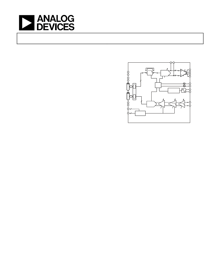
FUNCTIONAL BLOCK DIAGRAM
12
XTAL
RX–
4
6
AD9866
12
0 TO –7.5dB
0
0 TO –12dB
REGISTER
CONTROL
CLK
SYN.
ADC
80MSPS
2-4X
IOUT_G+
IOUT_N+
IOUT_N–
IOUT_G–
CLKOUT_1
CLKOUT_2
OSCIN
RX+
IAMP
TxDAC
I
I
2
M
CLK
MULTIPLIER
2-POLE
LPF
1-POLE
LPF
0 TO 6dB
= 1dB
– 6 TO 18dB
= 6dB
–6 TO 24dB
= 6dB
SPI
AGC[5:0]
RXCLK
RXE/SYNC
ADIO[11:6]/
Tx[5:0]
ADRx[5:0]
TXCLK
TXEN/SYNC
MODE
PWR DWN
Figure 1.
GENERAL DESCRIPTION
The AD9866 is a mixed-signal front end (MxFE) IC for
transceiver applications requiring Tx and Rx path functionality
with data rates up to 80 MSPS. Its flexible digital interface,
power saving modes, and high Tx-to-Rx isolation make it well
suited for half- and full-duplex applications. The digital inter-
face is extremely flexible allowing simple interfaces to digital
back ends that support half- or full-duplex data transfers, thus
often allowing the AD9866 to replace discrete ADC and DAC
solutions. Power saving modes include the ability to reduce
power consumption of individual functional blocks or to power
down unused blocks in half-duplex applications. A serial port
interface (SPI) allows software programming of the various
functional blocks. An on-chip PLL clock multiplier and
synthesizer provide all the required internal clocks, as well as
two external clocks from a single crystal or clock source.
The Tx signal path consists of a bypassable 2×/4× low-pass
interpolation filter, a 12-bit TxDAC, and a line driver. The
transmit path signal bandwidth can be as high as 34 MHz at an
input data rate of 80 MSPS. The TxDAC provides differential
current outputs that can be steered directly to an external load
or to an internal low distortion current amplifier. The current
amplifier (IAMP) can be configured as a current or voltage
mode line driver (with two external npn transistors) capable of
delivering in excess of 23 dBm peak signal power. Tx power can
be digitally controlled over a 19.5 dB range in 0.5 dB steps.
The receive path consists of a programmable amplifier
(RxPGA), a tunable low pass filter (LPF), and a 12-bit ADC. The
low noise RxPGA has a programmable gain range of 12 dB to
+48 dB in 1 dB steps. Its input referred noise is less than
3.3 nV/rtHz for gain settings beyond 30 dB. The receive path
LPF cutoff frequency can either be set over a 15 MHz to
35 MHz range or simply bypassed. The 12-bit ADC achieves
excellent dynamic performance over a 5 MSPS to 80 MSPS
span. Both the RxPGA and the ADC offer scalable power
consumption allowing power/performance optimization.
The AD9866 provides a highly integrated solution for many
broadband modems. It is available in a space-saving 64-lead
chip scale package and is specified over the commercial (40°C
to +85°C) temperature range.
相關PDF資料 |
PDF描述 |
|---|---|
| AD9866-EB | Broadband Modem Mixed Signal Front End |
| AD9866BCP | Broadband Modem Mixed Signal Front End |
| AD9870 | IF Digitizing Subsystem |
| AD9870EB | IF Digitizing Subsystem |
| AD9873 | Analog Front End Converter for Set-Top Box, Cable Modem |
相關代理商/技術參數 |
參數描述 |
|---|---|
| AD9866BCP | 制造商:Analog Devices 功能描述:Mixed Signal Front End 64-Pin LFCSP EP 制造商:Analog Devices 功能描述:12BIT MIXED SIGNAL CONVERTER 9866 |
| AD9866BCPRL | 制造商:Analog Devices 功能描述:Mixed Signal Front End 64-Pin LFCSP EP T/R |
| AD9866BCPZ | 功能描述:IC PROCESSOR FRONT END 64LFCSP RoHS:是 類別:RF/IF 和 RFID >> RF 前端 (LNA + PA) 系列:- 產品培訓模塊:Lead (SnPb) Finish for COTS Obsolescence Mitigation Program 標準包裝:250 系列:- RF 型:GPS 頻率:1575.42MHz 特點:- 封裝/外殼:48-TQFP 裸露焊盤 供應商設備封裝:48-TQFP 裸露焊盤(7x7) 包裝:托盤 |
| AD9866BCPZRL | 功能描述:IC PROCESSOR FRONT END 64LFCSP RoHS:是 類別:RF/IF 和 RFID >> RF 前端 (LNA + PA) 系列:- 產品培訓模塊:Lead (SnPb) Finish for COTS Obsolescence Mitigation Program 標準包裝:250 系列:- RF 型:GPS 頻率:1575.42MHz 特點:- 封裝/外殼:48-TQFP 裸露焊盤 供應商設備封裝:48-TQFP 裸露焊盤(7x7) 包裝:托盤 |
| AD9866CHIPS | 制造商:AD 制造商全稱:Analog Devices 功能描述:Broadband Modem Mixed Signal Front End |
發布緊急采購,3分鐘左右您將得到回復。