- 您現在的位置:買賣IC網 > PDF目錄373970 > AD9876BSTRL (ANALOG DEVICES INC) Broadband Modem Mixed-Signal Front End PDF資料下載
參數資料
| 型號: | AD9876BSTRL |
| 廠商: | ANALOG DEVICES INC |
| 元件分類: | 通信及網絡 |
| 英文描述: | Broadband Modem Mixed-Signal Front End |
| 中文描述: | SPECIALTY TELECOM CIRCUIT, PQFP48 |
| 封裝: | LQFP-48 |
| 文件頁數: | 18/24頁 |
| 文件大小: | 666K |
| 代理商: | AD9876BSTRL |
REV. A
AD9876
–18–
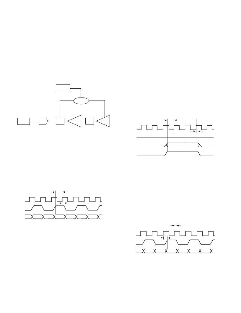
AGC TIMING CONSIDERATIONS
When implementing the AGC timing loop, it is important to
consider the delay and settling time of the Rx path in response
to a change in gain. Figure 4 shows the delay the receive signal
experiences through the blocks of the Rx path. Whether the gain
is programmed through the serial port or over the Tx [5:0] pins,
the gain takes effect immediately with the delays shown below.
When gain changes do not involve the CPGA, the new gain will
be evident in samples after seven ADC clock cycles. When the
gain change does involve the CPGA, it takes an additional 45ns
to 70 ns due to the propagation delays of the buffer, LPF and
PGA. Table V, details the PGA programming map.
5ns
GAIN
REGISTER
DECODE
LOGIC
DIGITAL
HPF
ADC
SHA
LPF
1 CLK
CYCLE
5 CLK
CYCLE
1/2 CLK
CYCLE
10ns
25ns or 50ns
10ns
PGA
BUFFER
Figure 4. AGC Timing
Transmit Port Timing
The AD9876 transmit port consists of a 6-bit databus Tx [5:0],
a clock, and a Tx SYNC signal. Two consecutive nibbles of the
Tx data are multiplexed together to form a 12-bit data-word.
The clock appearing on the CLK-A pin is a buffered version of
the internal Tx data sampling clock. Data from the Tx port is
read on the rising edge of this sampling clock. The Tx SYNC
signal is used to indicate to which word a nibble belongs. The
first nibble of every word is read while Tx SYNC is low, the
second nibble of that same word is read on the following Tx
SYNC high level. The timing is illustrated in the Figure 5.
Tx 2 LSB
Tx 3 MSB
Tx 1 LSB
Tx 2 MSB
Tx 0 LSB
Tx 1 MSB
t
SU
t
HD
CLK-A
Tx SYNC
Tx [5:0]
Figure 5. Transmit Timing Diagram AD9876
The Tx Port is highly configurable and offers the following options.
Negative edge sampling can be chosen by two different methods;
either by setting the Tx Port Negative Edge Sampling Bit (Reg-
ister 3, Bit 7) or the Invert
CLK-A Bit (Register 8, Bit 6). The
main difference between the two methods is that setting Register
3, Bit 7 inverts the internal sampling clock and will affect only
the transmit path, even if CLK-A is used to clock the Rx
data. However, inverting CLK-A would affect both the Rx and
Tx paths if they both use CLK-A.
The first nibble of each word can be read in as the least signifi
cant
nibble by setting the Tx LS Nibble First Bit (Register 7, Bit 2).
Also, the Tx path can be used in a Reduced Resolution Mode
by setting the Tx Port Multiplexer Bypass Bit (Register 7, Bit
0). In this mode, the Tx data-word becomes six bits and is read
in a single cycle. The clocking modes are the same as described
above, but the level of Tx SYNC is irrelevant.
If Tx SYNC is low for more than one clock cycle, the last trans-
mit data will read continuously until Tx SYNC is brought high
for the second nibble of a new transmit word. This feature can
be used to “flush” the interpolator filters with zeros.
PGA Adjust Timing
In addition to the serial port, the Tx [5:1] pins can be used to
write to the Rx Path Gain Adjust Bits (Register 6, Bits 4:0).
This provides a faster way to update the PGA gain. A high level
on the GAIN pin with Tx SYNC low programs the PGA setting
on either the rising edge or falling edge of CLK-A. The GAIN
pin must be held high, Tx SYNC must be held low, and GAIN
data must be stable for three clock cycles to successfully update
the PGA GAIN value. A low level on the GAIN pin enables data
to be fed to the interpolator and DAC.
t
SU
CLK-A
Tx SYNC
Tx [5:0]
t
HD
GAIN
GAIN
Figure 6. GAIN Programming
Receive Port Timing
The AD9876 receives port consists of a six bit databus Rx [5:0],
a clock, and an Rx SYNC signal. Two consecutive nibbles of the
Rx data are multiplexed together to form a 10-/12-bit data-word.
The Rx data is valid on the rising edge of CLK-A when the
ADC Clock Source
PLL-B/2 Bit (Register 3, Bit 6) is set to 0.
The Rx SYNC signal is used to indicate to which word a nibble
belongs. The first nibble of every word is transmitted while Rx
SYNC is low, the second nibble of that same word is transmit-
ted on the following Rx SYNC high level. When Rx SYNC is
low, the sampled nibble is read as the most significant nibble.
When the Rx SYNC is high, the sampled nibble is read as the
least significant nibble. The timing is illustrated in Figure 7.
t
VT
Rx 2 LSB
Rx 3 MSB
Rx 1 LSB
Rx 2 MSB
Rx 0 LSB
Rx 1 MSB
t
HT
CLK-A/-B
Rx SYNC
Rx [5:0]
Figure 7. Receive Timing Diagram
The Rx Port is highly configurable and offers the following
options.
Negative edge sampling can be chosen by setting the Invert
CLK-A Bit (Register 8, Bit 6) or the Invert CLK-B Bit (Register
8, Bit 7), depending on the clock selected as the ADC sampling
相關PDF資料 |
PDF描述 |
|---|---|
| AD9877 | Mixed-Signal Front End Set-Top Box, Cable Modem |
| AD9877ABS | Mixed-Signal Front End Set-Top Box, Cable Modem |
| AD9877-EB | Mixed-Signal Front End Set-Top Box, Cable Modem |
| AD9882KST-100 | Dual Interface for Flat Panel Displays |
| AD9882KST-140 | Dual Interface for Flat Panel Displays |
相關代理商/技術參數 |
參數描述 |
|---|---|
| AD9876EB | 制造商:Analog Devices 功能描述: |
| AD9876-EB | 制造商:AD 制造商全稱:Analog Devices 功能描述:Broadband Modem Mixed-Signal Front End |
| AD9877 | 制造商:AD 制造商全稱:Analog Devices 功能描述:Mixed-Signal Front End Set-Top Box, Cable Modem |
| AD9877ABS | 制造商:Rochester Electronics LLC 功能描述: 制造商:Analog Devices 功能描述: |
| AD9877ABS-1 | 制造商:Analog Devices 功能描述: |
發布緊急采購,3分鐘左右您將得到回復。