- 您現在的位置:買賣IC網 > PDF目錄373970 > AD9877 (Analog Devices, Inc.) Mixed-Signal Front End Set-Top Box, Cable Modem PDF資料下載
參數資料
| 型號: | AD9877 |
| 廠商: | Analog Devices, Inc. |
| 英文描述: | Mixed-Signal Front End Set-Top Box, Cable Modem |
| 中文描述: | 混合信號前端機頂盒,電纜調制解調器 |
| 文件頁數: | 27/36頁 |
| 文件大小: | 1094K |
| 代理商: | AD9877 |
第1頁第2頁第3頁第4頁第5頁第6頁第7頁第8頁第9頁第10頁第11頁第12頁第13頁第14頁第15頁第16頁第17頁第18頁第19頁第20頁第21頁第22頁第23頁第24頁第25頁第26頁當前第27頁第28頁第29頁第30頁第31頁第32頁第33頁第34頁第35頁第36頁
AD9877
Rev. B | Page 27 of 36
Q
X
Z
X
I
0
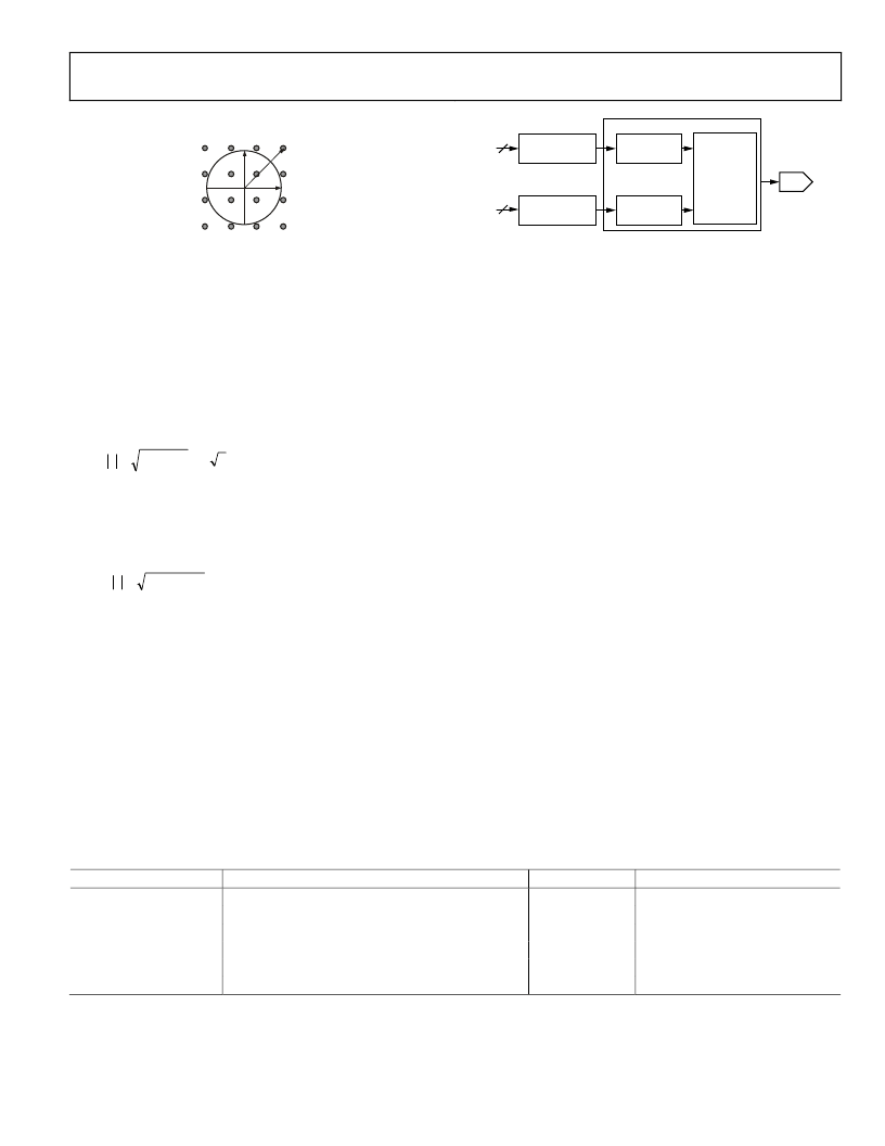
Figure 35. 16-Quadrature Modulation
Tx SIGNAL LEVEL CONSIDERATIONS
The quadrature modulator introduces a maximum gain of 3 dB
in the signal level. To visualize this, assume that both the I data
and Q data are fixed at the maximum possible digital value,
x
.
Then the output of the modulator,
z
, is
z
= [
x
cos(
ωt
)
x
sin(
ωt
)]
It can be shown that |
z
| assumes a maximum value of
(
2
=
+
=
x
x
x
z
)
(
)
dB
3
2
2
+
of
gain
a
However, if the same number of bits are used to represent the |
z
|
values as is used to represent the
x
values, an overflow occurs.
To prevent this possibility, an effective 3 dB attenuation is
internally implemented on the I and Q data path.
(
z
=
+
=
2
2
(
)
)
x
The following example assumes a Pk/rms level of 10 dB:
Maximum Symbol Component Input Value
=
±(2,047 LSBs 0.2 dB) = ±2,000 LSBs
Maximum Complex Input RMS Value
=
2,000 LSBs + 6 dB
Pk
/
rms
(dB) = 1,265 LSBs
rm
s
Maximum complex input rms value calculation uses both I and
Q symbol components, which adds a factor of 2 (6 dB) to the
formula.
Table 11 shows typical IQ input test signals with amplitude
levels related to 12-bit full scale (FS).
Table 11. IQ Input Test Signals
Analog Output
Digital Input
Single Tone (f
C
f)
I = cos(f)
Q = cos(f + 90°) = sin(f)
Single Tone (f
C
+ f)
I = cos(f)
Q = cos(f + 270°) = +sin(f)
Dual Tone (f
C
± f)
I = cos(f)
Q = cos(f + 180°) = cos(f) or Q = +cos(f)
ATTENUATOR
–3dB
MODULATOR
3dB MAX
I
O
O
I
ATTENUATOR
–3dB
TWOS COMPLEMENT FORMAT
HBF + CIC
INTERPOLATOR
+0.2dB
HBF + CIC
INTERPOLATOR
+0.2dB
12
12
I
O
COMPLEX DATA INPUT
DAC
0
Figure 36. Signal Level Contribution
Tx THROUGHPUT AND LATENCY
Data inputs impact the output fairly quickly but remain
effective due to the filter characteristics of the AD9877. Data
transmit latency through the AD9877 is easiest to describe in
terms of f
SYSCLK
clock cycles (4 f
MCLK
). The numbers quoted are
when an effect is first seen after an input value changes.
Latency of I/Q data entering the data assembler (AD9877 input)
to the DAC output is 119 f
SYSCLK
clock cycles (29.75 f
MCLK
cycles).
DC values applied to the data assembler input take up to 176
f
SYSCLK
clock cycles (44 f
MCLK
cycles) to propagate and settle at the
DAC output.
Frequency hopping is accomplished via changing the PROFILE
input pins. The time required to switch from one frequency to
another is less than 232 f
SYSCLK
cycles (58.5 f
MCLK
cycles).
DIGITAL-TO-ANALOG CONVERTER
A 12-bit digital-to-analog converter (DAC) is used to convert
the digitally processed waveform into an analog signal. The
worst-case spurious signals due to the DAC are the harmonics
of the fundamental signal and their aliases. The conversion
process produces aliased components of the fundamental signal
at
n
×
f
SYSCLK
±
f
CARRIER
(
n
= 1, 2, and 3). These are typically
filtered with an external RLC filter at the DAC output.
It is important for this analog filter to have a sufficiently flat
gain and linear phase response across the bandwidth of interest
to avoid modulation impairments. A relatively inexpensive
seventh-order elliptical low-pass filter is sufficient to suppress
the aliased components for HFC network applications.
Input Level
FS 0.2 dB
FS 0.2 dB
FS 0.2 dB
FS 0.2 dB
FS 0.2 dB
FS 0.2 dB
Modulator Output Level
FS 3.0 dB
FS 3.0 dB
FS
相關PDF資料 |
PDF描述 |
|---|---|
| AD9877ABS | Mixed-Signal Front End Set-Top Box, Cable Modem |
| AD9877-EB | Mixed-Signal Front End Set-Top Box, Cable Modem |
| AD9882KST-100 | Dual Interface for Flat Panel Displays |
| AD9882KST-140 | Dual Interface for Flat Panel Displays |
| AD9882 | Dual Interface for Flat Panel Displays |
相關代理商/技術參數 |
參數描述 |
|---|---|
| AD9877ABS | 制造商:Rochester Electronics LLC 功能描述: 制造商:Analog Devices 功能描述: |
| AD9877ABS-1 | 制造商:Analog Devices 功能描述: |
| AD9877ABSZ | 功能描述:IC PROCESSOR FRONT END 100MQFP RoHS:是 類別:集成電路 (IC) >> 數據采集 - 模擬前端 (AFE) 系列:- 產品培訓模塊:Lead (SnPb) Finish for COTS Obsolescence Mitigation Program 標準包裝:2,500 系列:- 位數:- 通道數:2 功率(瓦特):- 電壓 - 電源,模擬:3 V ~ 3.6 V 電壓 - 電源,數字:3 V ~ 3.6 V 封裝/外殼:32-VFQFN 裸露焊盤 供應商設備封裝:32-QFN(5x5) 包裝:帶卷 (TR) |
| AD9877BS | 制造商:Analog Devices 功能描述: |
| AD9877-EB | 制造商:Analog Devices 功能描述: |
發布緊急采購,3分鐘左右您將得到回復。