- 您現在的位置:買賣IC網 > PDF目錄373971 > AD9937 (Analog Devices, Inc.) CCD Signal Processor with Precision Timing⑩ Generator PDF資料下載
參數資料
| 型號: | AD9937 |
| 廠商: | Analog Devices, Inc. |
| 英文描述: | CCD Signal Processor with Precision Timing⑩ Generator |
| 中文描述: | CCD信號處理器精確定時⑩發生器 |
| 文件頁數: | 42/44頁 |
| 文件大小: | 410K |
| 代理商: | AD9937 |
第1頁第2頁第3頁第4頁第5頁第6頁第7頁第8頁第9頁第10頁第11頁第12頁第13頁第14頁第15頁第16頁第17頁第18頁第19頁第20頁第21頁第22頁第23頁第24頁第25頁第26頁第27頁第28頁第29頁第30頁第31頁第32頁第33頁第34頁第35頁第36頁第37頁第38頁第39頁第40頁第41頁當前第42頁第43頁第44頁
REV. 0
–42–
AD9937
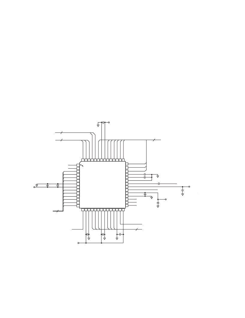
CIRCUIT LAYOUT INFORMATION
The AD9937 typical circuit connection is shown in Figure 41.
The PCB layout is critical in achieving good image quality from
the AD9937 product. All of the supply pins, particularly the
AVDD, DVDD, TCVDD, RSVDD, HVDD1, and HVDD2
supplies, must be decoupled to ground with good quality high
frequency chip capacitors. The decoupling capacitors should be
located as close as possible to the supply pins, and should have
a very low impedance path to a continuous ground plane. There
should also be a 4.7
μ
F or larger value bypass capacitor for each
main supply although this is not necessary for each individual pin.
In most applications, it is easier and recommended to share the
same supply for AVDD, DVDD, TCVDD, RSVDD, HVDD1,
and HVDD2, which may be done as long as the individual supply
pins are separately bypassed at each supply pin. A separate 3 V
supply should be used for DRVDD with this supply pin decoupled
to the same ground plane as the rest of the chip. A separate
ground for DRVSS is not recommended.
The analog bypass pins (REFB, REFT) should also be carefully
decoupled to ground as close as possible to their respective pins.
The analog input (CCDIN) capacitor should also be located
close to the pin.
The H1(A
–
D), H2(A, B), and RS printed circuit board traces
should be designed to have low inductance to avoid excessive distor-
tion of the signals. Heavier traces are recommended, because of
the large transient current demand on H1(A
–
D) and H2(A, B) by
the CCD. If possible, physically locate the AD9937 closer to the
CCD to reduce the inductance on these lines. As always, the rout-
ing path should be as direct as possible from the AD9937 to the
CCD. Careful trace impedance considerations must also be made
with applications using a flex printed circuit (FPC) connecting the
CCD to the AD9937. FPC trace impedances can be controlled
by applying a solid uniform ground plane under the H1(A
–
D),
H2(A, B), and RS traces. This helps minimize the amount of
overshoot and ringing on these signals at the CCD inputs.
36
35
34
33
32
31
30
29
37
39
38
42
41
40
15 16 17 18 19 20 21 22 23 24
25 26 27 28
1
2
3
4
5
6
7
8
9
10
11
12
13
14
48 47 46 45 44 43
PIN 1
IDENTIFIER
CCDIN
AVDD
D0
D1
D2
D3
D4
D5
D6
D7
D8
D9
AD9937
(TOP VIEW
10
DATA
OUTPUTS
3V
ANALOG SUPPLY
3V
DRIVER
SUPPLY
DRVDD
DRVSS
REFB
REFT
AVSS
VCKM
TCVDD
TCVSS
NC
V
H
R
V1A/B
V
V
O
V
TG1A
L
D
D
H
H
SERIAL
INTERFACE
4.7 F
8
OFD, LM, V4, TG3B, V3A/B,
TG3A, V2, TG1B, V1A/B, TG1A,
TO V-DRIVER
0.1 F
0.1 F
0.1 F
0.1 F
50
51
52
53
54
55
56
49
NC
NC
6
DATA OUTPUT CLOCK
3V ANALOG SUPPLY
0.1 F
0.1 F
0.1 F
H
H
R
R
H
H
H
H
H
NC
NC
H1D, H2B, H1B, H1C, H2A, H1A
RS
REF CLOCK INPUT
TG1B
T
T
S
S
S
3
2
V
H
4.7 F
0.1 F
CCD SIGNAL
3V ANALOG SUPPLY
VD, HD
1.0 F
1.0 F
3V ANALOG SUPPLY
Figure 41. Typical Circuit Configuration
相關PDF資料 |
PDF描述 |
|---|---|
| AD9937KCP | CCD Signal Processor with Precision Timing⑩ Generator |
| AD9937KCPRL | TVPS00RF-25-35PB W/ PC CONTACT |
| AD9942 | Dual-Channel, 14-Bit CCD Signal Processor with Precision Timing⑩ Core |
| AD9942BBCZ | Dual-Channel, 14-Bit CCD Signal Processor with Precision Timing⑩ Core |
| AD9942BBCZRL | Dual-Channel, 14-Bit CCD Signal Processor with Precision Timing⑩ Core |
相關代理商/技術參數 |
參數描述 |
|---|---|
| AD9937BCPZ-24 | 制造商:Analog Devices 功能描述: |
| AD9937BCPZ-27 | 功能描述:IC CCD SIGNAL PROC/GEN 制造商:analog devices inc. 系列:* 零件狀態:上次購買時間 標準包裝:1 |
| AD9937BCPZRL-24 | 制造商:Analog Devices 功能描述: |
| AD9937BCPZRL-27 | 功能描述:IC CCD SIGNAL PROC/GEN 制造商:analog devices inc. 系列:* 零件狀態:上次購買時間 標準包裝:1 |
| AD9937KCP | 制造商:Analog Devices 功能描述:AFE Video 1ADC 10-Bit 3V 56-Pin LFCSP EP 制造商:Rochester Electronics LLC 功能描述:- Bulk |
發布緊急采購,3分鐘左右您將得到回復。