- 您現(xiàn)在的位置:買賣IC網(wǎng) > PDF目錄373972 > AD9957_07 (Analog Devices, Inc.) 1 GSPS Quadrature Digital Upconverter with 18-Bit IQ Data Path and 14-Bit DAC PDF資料下載
參數(shù)資料
| 型號(hào): | AD9957_07 |
| 廠商: | Analog Devices, Inc. |
| 英文描述: | 1 GSPS Quadrature Digital Upconverter with 18-Bit IQ Data Path and 14-Bit DAC |
| 中文描述: | 1 GSPS的正交數(shù)字上變頻器與18位智商數(shù)據(jù)路徑和14位DAC |
| 文件頁(yè)數(shù): | 41/60頁(yè) |
| 文件大小: | 840K |
| 代理商: | AD9957_07 |
第1頁(yè)第2頁(yè)第3頁(yè)第4頁(yè)第5頁(yè)第6頁(yè)第7頁(yè)第8頁(yè)第9頁(yè)第10頁(yè)第11頁(yè)第12頁(yè)第13頁(yè)第14頁(yè)第15頁(yè)第16頁(yè)第17頁(yè)第18頁(yè)第19頁(yè)第20頁(yè)第21頁(yè)第22頁(yè)第23頁(yè)第24頁(yè)第25頁(yè)第26頁(yè)第27頁(yè)第28頁(yè)第29頁(yè)第30頁(yè)第31頁(yè)第32頁(yè)第33頁(yè)第34頁(yè)第35頁(yè)第36頁(yè)第37頁(yè)第38頁(yè)第39頁(yè)第40頁(yè)當(dāng)前第41頁(yè)第42頁(yè)第43頁(yè)第44頁(yè)第45頁(yè)第46頁(yè)第47頁(yè)第48頁(yè)第49頁(yè)第50頁(yè)第51頁(yè)第52頁(yè)第53頁(yè)第54頁(yè)第55頁(yè)第56頁(yè)第57頁(yè)第58頁(yè)第59頁(yè)第60頁(yè)
AD9957
which three AD9957s are synchronized with one device operating
as a master timing unit and the others as slave units.
Rev. 0 | Page 41 of 60
The master device must have its SYNC_IN pins included as part
of the synchronization distribution and delay equalization mecha-
nism for it to be synchronized with the slave units.
The synchronization mechanism begins with the clock distribu-
tion and delay equalization block, which ensures that all devices
receive an edge aligned REFCLK signal. However, even though
the REFCLK signal is edge aligned among all devices, this alone
does not guarantee that the clock state of each internal clock
generator is coordinated with the others. This is the role of the
synchronization and delay equalization block. This block accepts
the SYNC_OUT signal generated by the master device and
redistributes it to the SYNC_IN input of the slave units (as well
as feeding it back to the master). The goal of the redistributed
SYNC_OUT signal from the master device is to deliver an edge
aligned SYNC_IN signal to all of the sync receivers.
Assuming that all devices share the same REFCLK edge (due to
the clock distribution and delay equalization block) and that all
devices share the same SYNC_IN edge (due to the synchroniza-
tion and delay equalization block), then all devices should be
generating an internal sync pulse in unison (assuming they all
have the same sync receiver delay value). With the further
stipulation that all devices have the same sync state preset value,
then the synchronized sync pulses cause all of the devices to
assume the same predefined clock state simultaneously. That is,
the internal clocks of all devices are fully synchronized.
The synchronization mechanism depends on the reliable
generation of a sync pulse by the edge detection block in the
sync receiver. Generation of a valid sync pulse, however,
requires proper sampling of the rising edge of the delayed
sync-in signal with the rising edge of the local SYSCLK. If the
edge timing of these signals fails to meet the setup or hold time
requirements of the internal latches in the edge detection
circuitry, then the proper generation of the sync pulse is in
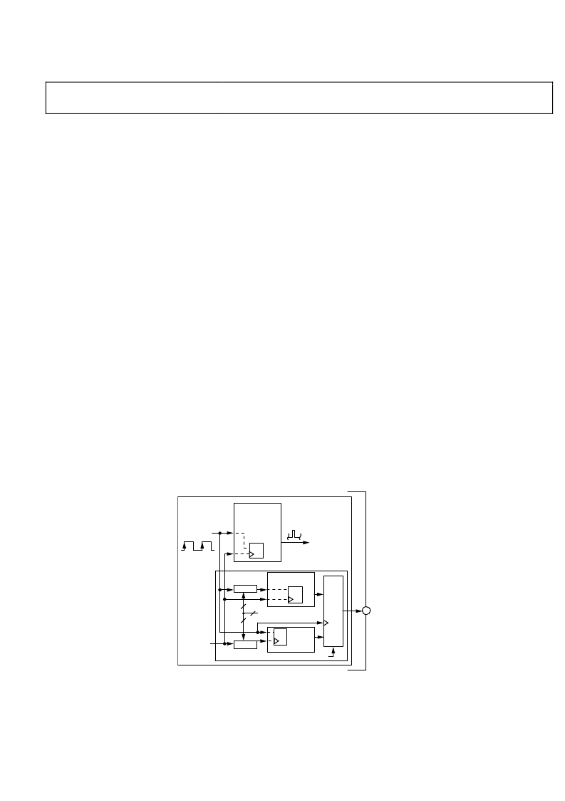
jeopardy. The setup-and-hold validation block (see Figure 58)
gives the user a means to validate that proper edge timing exists
between the two signals. The setup-and-hold validation block
can be disabled via the sync timing validation disable bit in Control
Function Register 2.
The validation block makes use of a user-specified time window
(programmable in increments of ~150 ps via the 4-bit sync
validation delay word in the multichip sync register). The setup
validation and hold validation circuits use latches identical to
those in the rising edge detector and strobe generator. The
programmable time window is used to skew the timing between
the rising edges of the local SYSCLK signal and the rising edges
of the delayed sync-in signal. If either the hold or setup valida-
tion circuits fail to detect a valid edge sample, the condition is
indicated externally via the SYNC_SMP_ERR pin (active high).
The user must choose a sync validation delay value that is a
reasonable fraction of the SYSCLK period. For example, if the
SYSCLK frequency is 1 GHz (1 ns period), then a reasonable
value is 1 or 2 (150 ps or 300 ps). Choosing too large a value can
cause the SYNC_SMP_ERR pin to generate false error signals.
Choosing too small a value may cause instability.
SYNC
PULSE
SYSCLK
DELAY
DELAY
C
4
SYNC VALIDATION
DELAY
4
4
SYNC_SMP_ERR
SYNC RECEIVER
12
SYNC TIMING VALIDATION DISABLE
SETUP
VALIDATION
HOLD
VALIDATION
D Q
SETUP AND HOLD VALIDATION
TO
CLOCK
GENERATION
LOGIC
FROM
SYNC
RECEIVER
DELAY
LOGIC
D Q
D Q
RISING EDGE
DETECTOR
AND STROBE
GENERATOR
0
Figure 58. Sync Timing Validation Block
相關(guān)PDF資料 |
PDF描述 |
|---|---|
| AD9958BCPZ-REEL7 | 2-Channel 500 MSPS DDS with 10-Bit DACs |
| AD9958 | 2-Channel 500 MSPS DDS with 10-Bit DACs |
| AD9958BCPZ | 2-Channel 500 MSPS DDS with 10-Bit DACs |
| AD9970 | 14-Bit CCD Signal Processor with Precision Timing Generator |
| AD9971 | 12-Bit CCD Signal Processor with Precision Timing |
相關(guān)代理商/技術(shù)參數(shù) |
參數(shù)描述 |
|---|---|
| AD9957BCPZ | 制造商:Analog Devices 功能描述:GSPS QUADRATURE DIGITAL UPCONVERTER W/18-BIT IQ DATA PATH - Trays |
| AD9957BSVZ | 功能描述:IC DDS 1GSPS 14BIT IQ 100TQFP RoHS:是 類別:集成電路 (IC) >> 接口 - 直接數(shù)字合成 (DDS) 系列:- 產(chǎn)品變化通告:Product Discontinuance 27/Oct/2011 標(biāo)準(zhǔn)包裝:2,500 系列:- 分辨率(位):10 b 主 fclk:25MHz 調(diào)節(jié)字寬(位):32 b 電源電壓:2.97 V ~ 5.5 V 工作溫度:-40°C ~ 85°C 安裝類型:表面貼裝 封裝/外殼:16-TSSOP(0.173",4.40mm 寬) 供應(yīng)商設(shè)備封裝:16-TSSOP 包裝:帶卷 (TR) |
| AD9957BSVZ-REEL | 功能描述:IC DDS 1GSPS 14BIT IQ 100TQFP RoHS:是 類別:集成電路 (IC) >> 接口 - 直接數(shù)字合成 (DDS) 系列:- 產(chǎn)品變化通告:Product Discontinuance 27/Oct/2011 標(biāo)準(zhǔn)包裝:2,500 系列:- 分辨率(位):10 b 主 fclk:25MHz 調(diào)節(jié)字寬(位):32 b 電源電壓:2.97 V ~ 5.5 V 工作溫度:-40°C ~ 85°C 安裝類型:表面貼裝 封裝/外殼:16-TSSOP(0.173",4.40mm 寬) 供應(yīng)商設(shè)備封裝:16-TSSOP 包裝:帶卷 (TR) |
| AD9957BSVZREEL13 | 制造商:AD 制造商全稱:Analog Devices 功能描述:1 GSPS Quadrature Digital Upconverter w/18-Bit IQ Data Path and 14-Bit DAC |
| AD9958 | 制造商:AD 制造商全稱:Analog Devices 功能描述:2-Channel 500 MSPS DDS with 10-Bit DACs |
發(fā)布緊急采購(gòu),3分鐘左右您將得到回復(fù)。