- 您現在的位置:買賣IC網 > PDF目錄373983 > ADF4251 (Analog Devices, Inc.) Dual Fractional-N/Integer-N Frequency Synthesizer PDF資料下載
參數資料
| 型號: | ADF4251 |
| 廠商: | Analog Devices, Inc. |
| 英文描述: | Dual Fractional-N/Integer-N Frequency Synthesizer |
| 中文描述: | 雙Fractional-N/Integer-N頻率合成器 |
| 文件頁數: | 11/28頁 |
| 文件大小: | 387K |
| 代理商: | ADF4251 |
第1頁第2頁第3頁第4頁第5頁第6頁第7頁第8頁第9頁第10頁當前第11頁第12頁第13頁第14頁第15頁第16頁第17頁第18頁第19頁第20頁第21頁第22頁第23頁第24頁第25頁第26頁第27頁第28頁
REV. 0
ADF4251
–11–
CIRCUIT DESCRIPTION
Reference Input Section
The reference input stage is shown in Figure 3. SW1 and SW2
are normally closed switches. SW3 is normally open. When
power-down is initiated, SW3 is closed and SW1 and SW2 are
opened. This ensures that there is no loading of the REF
IN
pin
on power-down.
POWER-DOWN
CONTROL
REF
IN
NC
NC
NO
SW3
SW2
SW1
100k
BUFFER
TO R
COUNTER
NC = NORMALLY CLOSED
NO = NORMALLY OPEN
REF
OUT
XOEB
Figure 3. Reference Input Stage
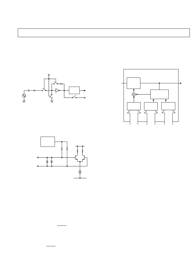
RF and IF Input Stage
The RF input stage is shown in Figure 4. The IF input stage is
the same. It is followed by a two-stage limiting amplifier to
generate the CML clock levels needed for the N counter.
2k
2k
1.6V
BIAS
GENERATOR
RF
IN
A
RF
IN
B
V
DD
1
A
GND
Figure 4. RF Input Stage
RF INT Divider
The RF INT CMOS counter allows a division ratio in the PLL
feedback counter. Division ratios from 31 to 255 are allowed.
INT, FRAC, MOD, and R Relationship
The INT, FRAC, and MOD values, in conjunction with the
RF R counter, make it possible to generate output frequencies
that are spaced by fractions of the RF phase frequency detector
(PFD). The equation for the RF VCO frequency (
RF
OUT
) is
RF
F
INT
FRAC
MOD
OUT
PFD
=
¥
+
ê
ˉ
(1)
where
RF
OUT
is the output frequency of external voltage controlled
oscillator (VCO).
(
F
REF
D
R
PFD
IN
=
¥
+
)
1
(2)
REF
IN
= the reference input frequency,
D
= RF REF
IN
Doubler
Bit,
R
= the preset divide ratio of the binary 4-bit program-
mable reference counter (1 to 15),
INT
= the preset divide ratio of
the binary 8-bit counter (31 to 255),
MOD
= the preset modulus
ratio of binary 12-bit programmable FRAC counter (2 to 4095),
and
FRAC
= the preset fractional ratio of the binary 12-bit
programmable FRAC counter (0 to MOD).
N = INT + FRAC/MOD
FROM RF
INPUT STAGE
TO PFD
RF N DIVIDER
THIRD-ORDER
FRACTIONAL
INTERPOLATOR
MOD
REG
INT
REG
FRAC
VALUE
N-COUNTER
Figure 5. N Counter
RF R Counter
The 4-bit RF R counter allows the input reference frequency
(REF
IN
) to be divided down to produce the reference clock to
the RF PFD. Division ratios from 1 to 15 are allowed.
IF R Counter
The 15-bit IF R counter allows the input reference frequency
(REF
IN
) to be divided down to produce the reference clock to
the IF PFD. Division ratios from 1 to 32767 are allowed.
IF Prescaler (P/P + 1)
The dual modulus IF prescaler (P/P + 1), along with the IF A
and B counters, enables the large division ratio, N, to be realized
(N = PB + A). Operating at CML levels, it takes the clock from
the IF input stage and divides it down to a manageable frequency
for the CMOS IF A and CMOS IF B counters.
IF A and B Counters
The IF A CMOS and IF B CMOS counters combine with the
dual modulus IF prescaler to allow a wide ranging division ratio
in the PLL feedback counter. The counters are guaranteed to
work when the prescaler output is 150 MHz or less.
Pulse Swallow Function
The IF A and IF B counters, in conjunction with the dual modulus
IF prescaler, make it possible to generate output frequencies
that are spaced only by the reference frequency divided by R.
See the Device Programming after Initial Power-Up section for
examples. The equation for the IF VCO (
IF
OUT
) frequency is
(
where
IF
OUT
= the output frequency of the external voltage controlled
oscillator (VCO),
P
= the preset modulus of the IF dual modulus
prescaler,
B
= the preset divide ratio of the binary 12-bit counter
(3 to 4095), and
A
= the preset divide ratio of the binary 6-bit
swallow counter (0 to 63).
F
PFD
is obtained using Equation 2.
IF
P
B
A
F
OUT
PFD
=
¥
)
+
[
]
¥
(3)
相關PDF資料 |
PDF描述 |
|---|---|
| ADF4251BCP | Dual Fractional-N/Integer-N Frequency Synthesizer |
| ADF4251BCP-REEL | Dual Fractional-N/Integer-N Frequency Synthesizer |
| ADF4251BCP-REEL7 | Dual Fractional-N/Integer-N Frequency Synthesizer |
| ADF4252BCP | Dual Fractional-N/Integer-N Frequency Synthesizer |
| ADF4252BCP-REEL | Dual Fractional-N/Integer-N Frequency Synthesizer |
相關代理商/技術參數 |
參數描述 |
|---|---|
| ADF4251BCP | 制造商:Analog Devices 功能描述:PLL Frequency Synthesizer Dual 24-Pin LFCSP EP |
| ADF4251BCP-REEL | 制造商:AD 制造商全稱:Analog Devices 功能描述:Dual Fractional-N/Integer-N Frequency Synthesizer |
| ADF4251BCP-REEL7 | 制造商:AD 制造商全稱:Analog Devices 功能描述:Dual Fractional-N/Integer-N Frequency Synthesizer |
| ADF4252 | 制造商:AD 制造商全稱:Analog Devices 功能描述:Dual Fractional-N/Integer-N Frequency Synthesizer |
| ADF4252BCP | 制造商:Analog Devices 功能描述:PLL Frequency Synthesizer Dual 24-Pin LFCSP EP 制造商:Rochester Electronics LLC 功能描述:1000-2500MHZ FRAC-N PLL - Bulk 制造商:Analog Devices 功能描述:IC SYNTHESIZER PLL |
發布緊急采購,3分鐘左右您將得到回復。