- 您現(xiàn)在的位置:買賣IC網(wǎng) > PDF目錄373983 > ADF4251 (Analog Devices, Inc.) Dual Fractional-N/Integer-N Frequency Synthesizer PDF資料下載
參數(shù)資料
| 型號: | ADF4251 |
| 廠商: | Analog Devices, Inc. |
| 英文描述: | Dual Fractional-N/Integer-N Frequency Synthesizer |
| 中文描述: | 雙Fractional-N/Integer-N頻率合成器 |
| 文件頁數(shù): | 25/28頁 |
| 文件大小: | 387K |
| 代理商: | ADF4251 |
第1頁第2頁第3頁第4頁第5頁第6頁第7頁第8頁第9頁第10頁第11頁第12頁第13頁第14頁第15頁第16頁第17頁第18頁第19頁第20頁第21頁第22頁第23頁第24頁當前第25頁第26頁第27頁第28頁
REV. 0
ADF4251
–25–
IF Side Not In Use
If the IF side is not being used, the following pinout is recom-
mended for the IF side:
Pin No.
Mnemonic
Description
14
15
A
GND
2
IF
IN
B
Short to all other ground pins.
Leave open circuit. (This is biased
up to V
DD
/2 internally.)
Leave open circuit. (This is biased
up to V
DD
/2 internally.)
Leave open circuit. (This is internally
three-stated until power-up.)
Short to V
P
1. (V
P
1 is the RF CP
supply.)
Short to V
DD
1 (V
DD
1 is the RF V
DD
supply.)
16
IF
IN
A
19
CP_IF
20
V
P
2
21
V
DD
2
INTERFACING
The ADF4251 has a simple SPI compatible serial interface for
writing to the device. SCLK, SDATA, and LE control the data
transfer. When LE (Latch Enable) goes high, the 24 bits that have
been clocked into the input register on each rising edge of SCLK
will be transferred to the appropriate latch. See Figure 1 for the
Timing Diagram and Table I for the Control Bit Truth Table.
The maximum allowable serial clock rate is 20 MHz. This means
that the maximum update rate possible for the device is 833 kHz
or one update every 1.2 μs. This is certainly more than adequate
for systems that will have typical lock times in hundreds of
microseconds.
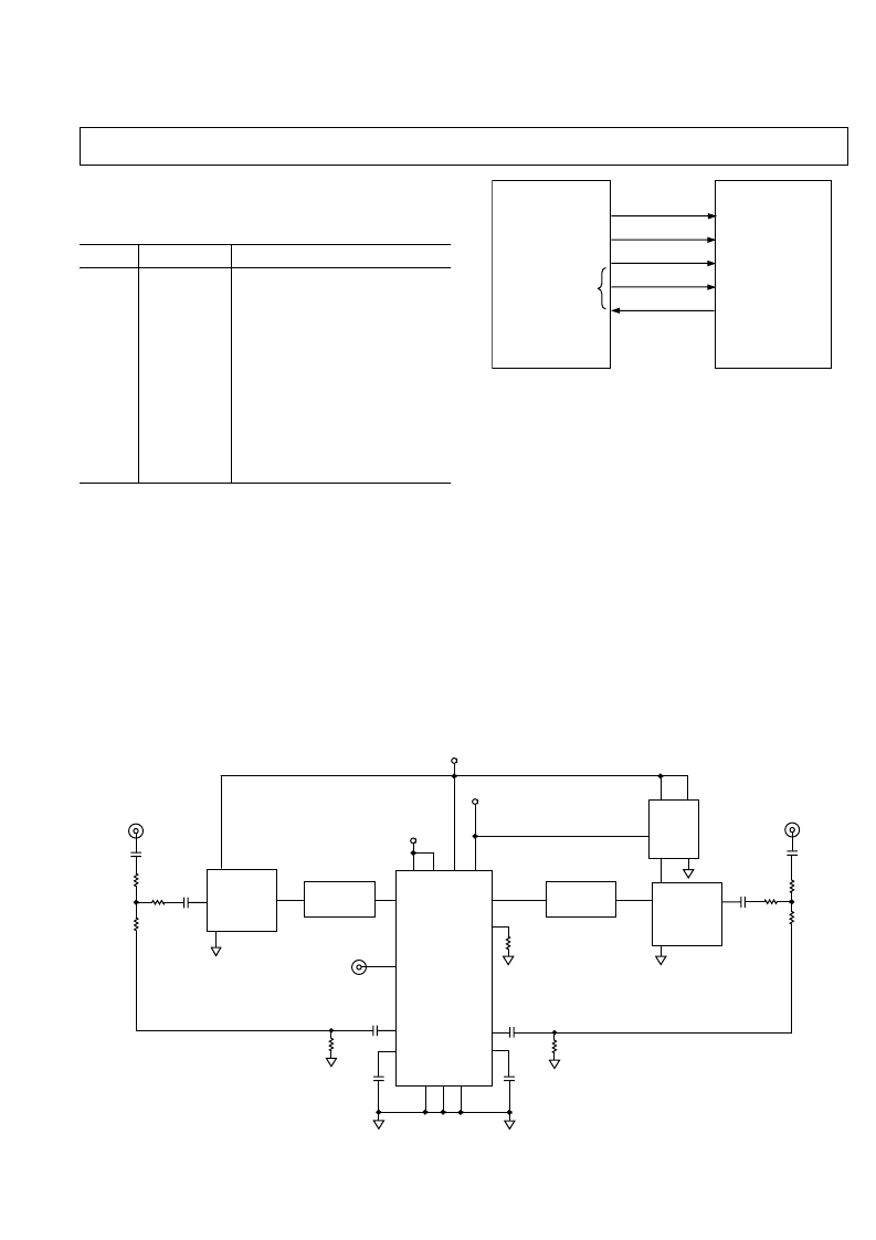
ADuC812
ADF4251
SCLK
SDATA
LE
CE
MUXOUT
(LOCK DETECT)
SCLOCK
MOSI
I/O PORTS
Figure 8. ADuC812 to ADF4251 Interface
ADuC812 Interface
Figure 8 shows the interface between the ADF4251 and the
ADuC812 microconverter. Since the ADuC812 is based on
an 8051 core, this interface can be used with any 8051-based
microcontroller. The microconverter is set up for SPI Master
mode with CPHA = 0. To initiate the operation, the I/O port
driving LE is brought low. Each latch of the ADF4251 needs
(at most) a 24-bit word. This is accomplished by writing three
8-bit bytes from the microconverter to the device. When the third
byte has been written, the LE input should be brought high to
complete the transfer.
I/O port lines on the ADuC812 are also used to control power-
down (CE input) and to detect lock (MUXOUT configured as
lock detect and polled by the port input).
When operating in the mode described, the maximum SCLOCK
rate of the ADuC812 is 4 MHz. This means that the maximum
rate at which the output frequency can be changed will be 166 kHz.
RF VCO
V
CC
RF LOOP
FILTER
GND
ADF4251
RF
OUT
100pF
100pF
18
18
18
DECOUPLING CAPACITORS AND INTERFACE SIGNALS
HAVE BEEN OMITTED FROM THE DIAGRAM IN THE
INTERESTS OF GREATER CLARITY.
51
100pF
100pF
RF
IN
A
RF
IN
B
REF
IN
REFIN
V
DD
V
P
CE
V
DD
DV
DD
V
P
RF CP
C
G
A
G
D
G
2.7k
POWER-DOWN CONTROL
ADG702
IN
D
S
V
DD
GND
R
SET
IF
OUT
100pF
100pF
18
18
18
IF VCO
V
CC
GND
IF LOOP
FILTER
51
100pF
100pF
IF
IN
A
IF
IN
B
IF CP
Figure 9. Power-Down Circuit
相關PDF資料 |
PDF描述 |
|---|---|
| ADF4251BCP | Dual Fractional-N/Integer-N Frequency Synthesizer |
| ADF4251BCP-REEL | Dual Fractional-N/Integer-N Frequency Synthesizer |
| ADF4251BCP-REEL7 | Dual Fractional-N/Integer-N Frequency Synthesizer |
| ADF4252BCP | Dual Fractional-N/Integer-N Frequency Synthesizer |
| ADF4252BCP-REEL | Dual Fractional-N/Integer-N Frequency Synthesizer |
相關代理商/技術參數(shù) |
參數(shù)描述 |
|---|---|
| ADF4251BCP | 制造商:Analog Devices 功能描述:PLL Frequency Synthesizer Dual 24-Pin LFCSP EP |
| ADF4251BCP-REEL | 制造商:AD 制造商全稱:Analog Devices 功能描述:Dual Fractional-N/Integer-N Frequency Synthesizer |
| ADF4251BCP-REEL7 | 制造商:AD 制造商全稱:Analog Devices 功能描述:Dual Fractional-N/Integer-N Frequency Synthesizer |
| ADF4252 | 制造商:AD 制造商全稱:Analog Devices 功能描述:Dual Fractional-N/Integer-N Frequency Synthesizer |
| ADF4252BCP | 制造商:Analog Devices 功能描述:PLL Frequency Synthesizer Dual 24-Pin LFCSP EP 制造商:Rochester Electronics LLC 功能描述:1000-2500MHZ FRAC-N PLL - Bulk 制造商:Analog Devices 功能描述:IC SYNTHESIZER PLL |
發(fā)布緊急采購,3分鐘左右您將得到回復。